Products


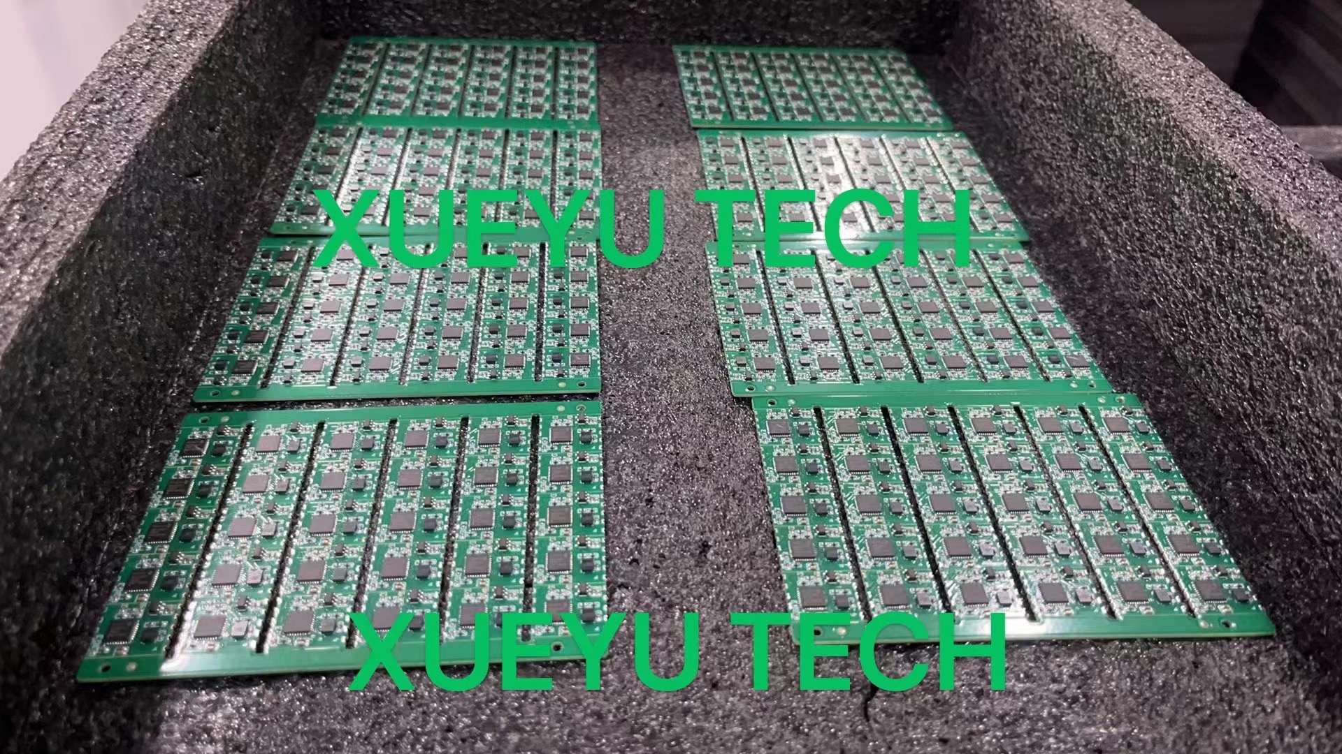


Hot Sales
 Industrial Automation and Controls
  Filters
  Inductors, Coils, Chokes
  Potentiometers, Variable Resistors
  Optoelectronics
  Power Supplies - External/Internal (Off-Board)
  Circuit Protection


Brand


News
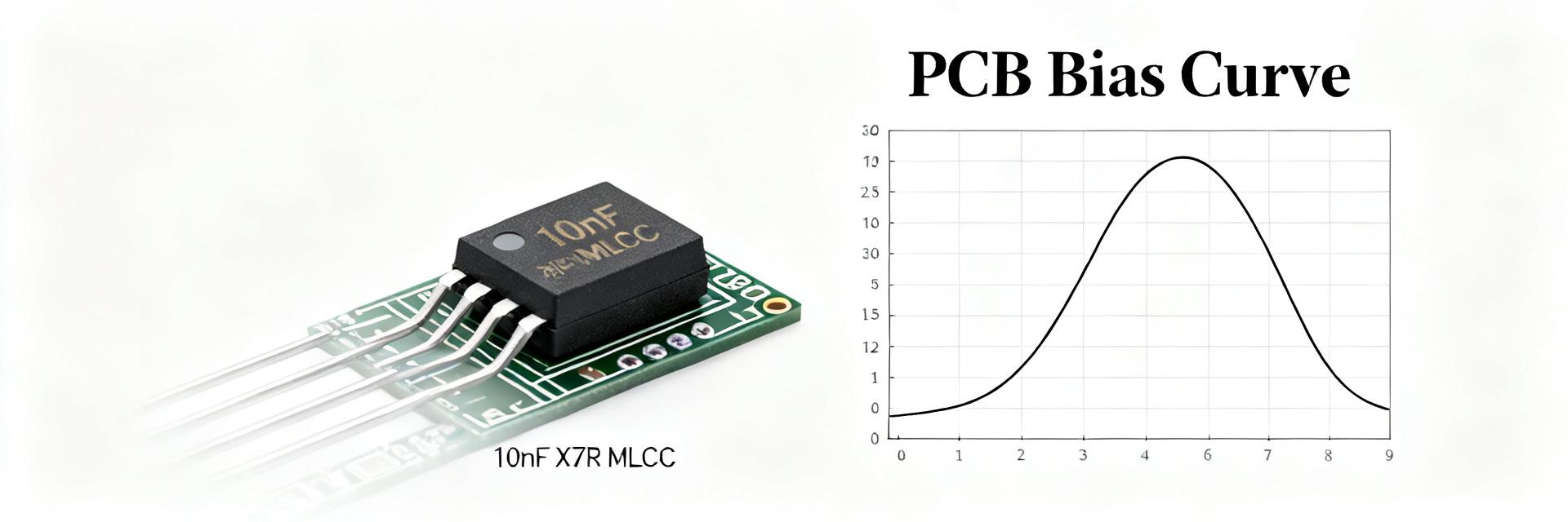
10nF 25V X7R MLCC: Performance Data & Failure Rates
Reliability audits and accelerated-life test insights for precision engineering. In recent reliability audits and accelerated-life tests, 10nF 25V X7R MLCC parts show wide variatio…
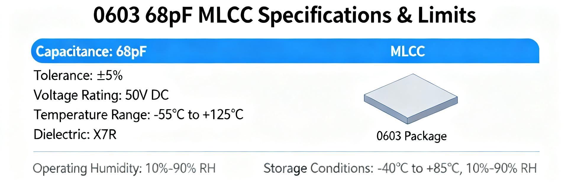
06033A680K4T2A datasheet: key specs, test data & limits
Bench testing of comparable 0603 MLCCs shows many failure modes and parameter drift emerging above 85°C and in high-humidity conditions, so reading the 06033A680K4T2A datasheet car…
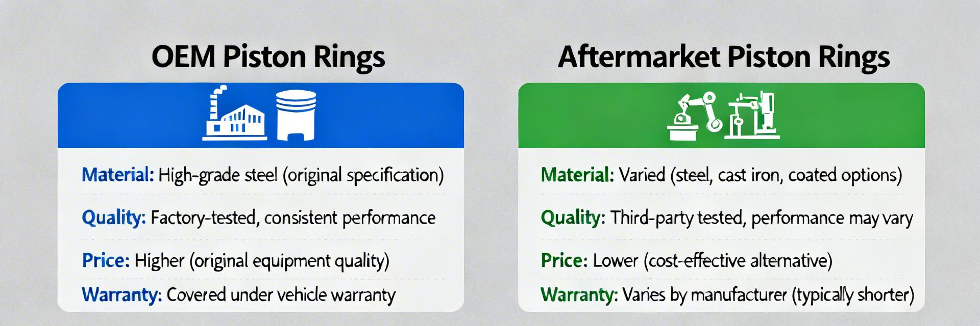
Piston Rings Cost Breakdown: OEM vs Aftermarket Insights
🚀 Key Takeaways ✅ Total Budget: Expect $1,000–$5,000 for full replacement including labor/machining. ✅ OEM Advantage: Guarantees factory tolerances and preserves vehicle warranty. …
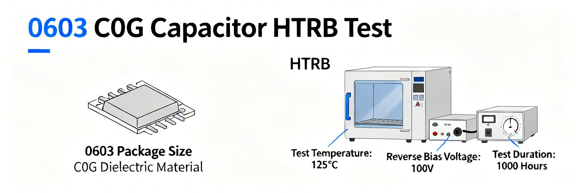
06033A120K4T2A Reliability Report: Test Data & Specs
Key Takeaways (Reliability Insights) Proven Longevity: 99.1% survival rate under 1,000-hour HTRB stress ensures a 15+ year automotive service life. Precision Stability: Minimal 0.4…
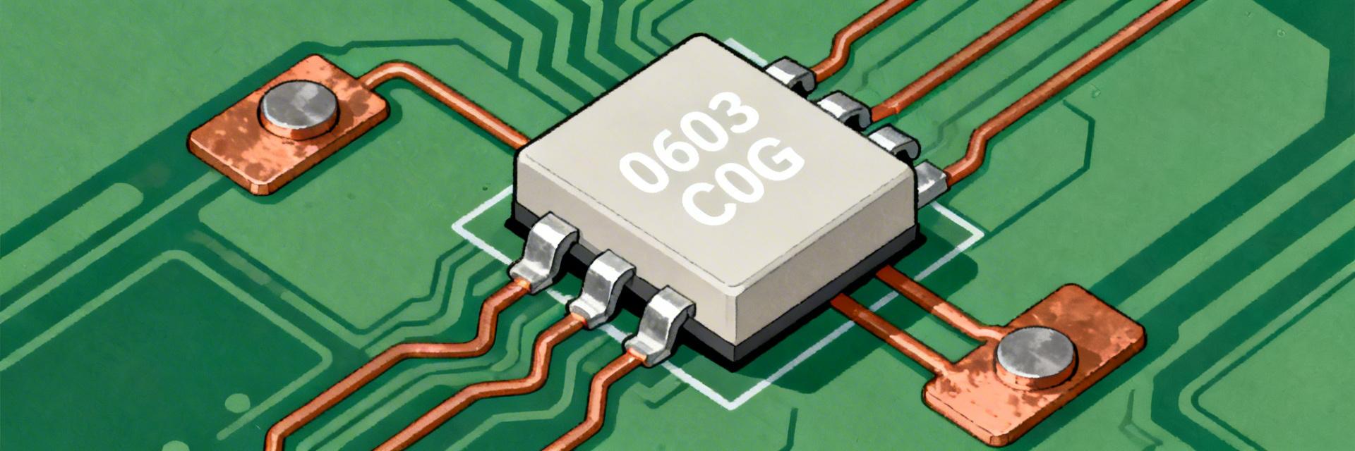
06033A101K4T2A Datasheet: Specs, Footprint Tips & PCB Layout
Key Takeaways for Engineers Ultra-Stable C0G: Zero capacitance drift ensures precision in RF and timing circuits. 25V Safety Margin: High voltage headroom provides 2x reliability o…
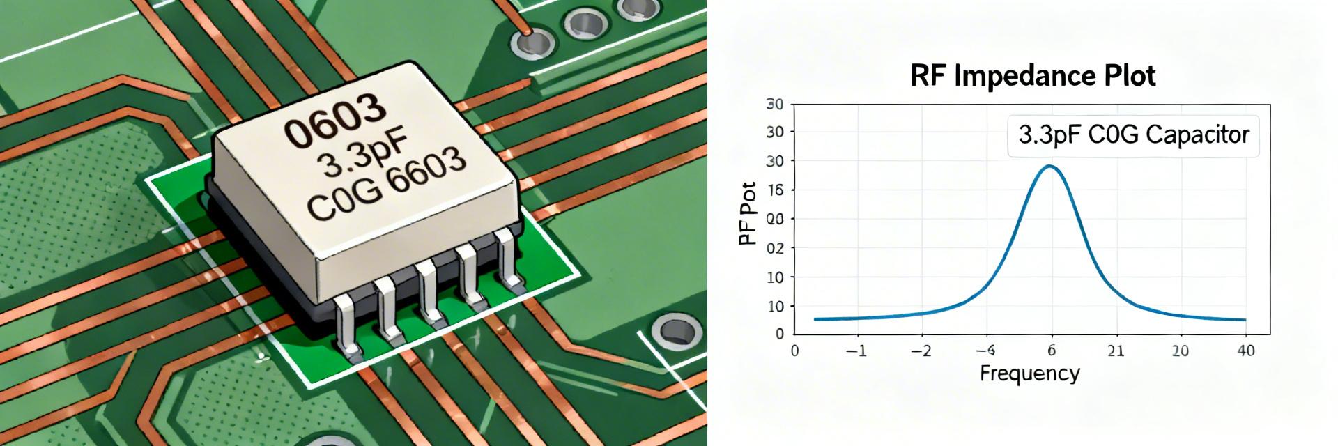
06032U3R3BAT2A capacitor: Deep Specs & Test Data Reviewed
Key Takeaways Ultra-Stable Tuning: 3.3pF C0G dielectric ensures zero aging and ±0.1pF precision for RF filters. High Voltage Margin: 200V rating provides 4x safety overhead compare…
