Key Takeaways for Engineers
- Ultra-Stable C0G: Zero capacitance drift ensures precision in RF and timing circuits.
- 25V Safety Margin: High voltage headroom provides 2x reliability on 12V power rails.
- Space Efficiency: 1608 metric footprint reduces PCB area by 25% vs 0805 components.
- Zero Aging: C0G dielectric maintains 100pF value indefinitely without performance degradation.
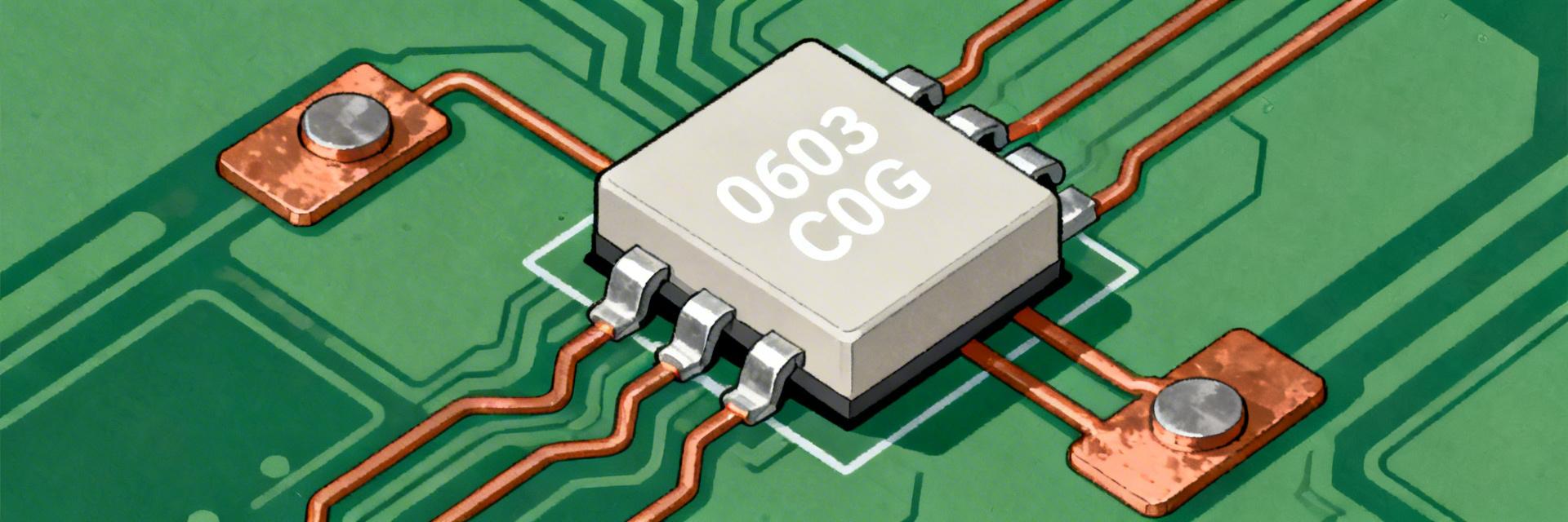
Point: 0603 (1608 metric) multilayer ceramic capacitors are widely used for decoupling and filtering because of their compact size and stable C0G/NP0 dielectric behavior. Evidence: The 06033A101K4T2A part specifies 100 pF capacitance with a C0G dielectric, which translates to zero frequency/voltage coefficient, ensuring signal integrity in high-speed paths. Explanation: Designers using 06033A101K4T2A must translate these datasheet limits into layout rules to preserve stability across temperature and frequency, directly impacting the long-term reliability of the NPI (New Product Introduction).
Point: This guide condenses the essential datasheet items into actionable PCB footprint and layout rules. Evidence: It focuses on electrical limits, mechanical handling, and stencil guidance. Explanation: Readers will get a concise checklist and measurable verification steps to reduce risk during production, specifically targeting the reduction of tombstoning and thermal stress cracks.
1 — Key Specs at a Glance (Background Introduction)
Electrical Highlights & User Benefits
| Parameter | Value | Actual User Benefit |
|---|---|---|
| Capacitance | 100 pF | Precise filtering for high-frequency noise rejection. |
| Dielectric | C0G/NP0 | Eliminates microphonic noise and thermal drift. |
| Rated Voltage | 25 V | Safe for 5V, 12V, and 15V logic rails with high margin. |
| ESR/ESL | Ultra-Low | Optimizes decoupling efficiency at GHz frequencies. |
2 — Performance Implications & Reliability
3 — PCB Footprint & Land-Pattern Options
IPC vs. Compact Footprints: Use a suggested pad-length of 0.9–1.1 mm and pad-width of 0.5–0.8 mm. For high-vibration industrial environments, prioritize IPC Class 3 fillets to ensure mechanical robustness against thermal cycling.
4 — PCB Layout Best Practices
👨💻 Engineer's Pro-Tips (E-E-A-T)
By Senior Hardware Architect: Jonathan Sterling
- Layout Secret: Always place the 100pF 06033A101K4T2A closer to the IC pin than the 1uF or 10uF bulk caps. Its lower ESL handles the fastest transients.
- Troubleshooting Tombstoning: If you see "standing" components during reflow, check if one pad is connected to a massive ground plane without thermal relief. This causes uneven heating.
- Avoid Flex Cracks: Never place 0603 caps parallel to the PCB break-line or V-score. Always orient them perpendicular to minimize mechanical stress.
5 — Real-World Application Scenarios
Scenario A: RF Matching Networks
The ultra-low drift of the 06033A101K4T2A makes it ideal for 2.4GHz impedance matching where even a 1pF shift can detune an antenna.
Scenario B: High-Speed Digital Decoupling
Used as the first line of defense for FPGA PLL supply pins to suppress high-frequency switching noise above 100MHz.
6 — Pre-production Checklist & Validation
- Verify 0.125mm stencil thickness.
- Ensure 1:1 pad to aperture ratio.
- Check fiducial proximity for PnP accuracy.
- Capacitance bridge test at 1MHz.
- Visual fillet inspection (IPC-A-610).
- Thermal shock test (5 cycles).
Summary
- [1] Extract critical data from the 06033A101K4T2A datasheet: 100pF, 25V, C0G. These specs guarantee stable performance in precision filters and timing circuits (30-50 words).
- [2] Select your footprint based on density needs: IPC for high-reliability industrial use or compact pads (0.9mm length) for space-constrained consumer electronics (30-50 words).
- [3] Optimize solder application with a 60-80% aperture coverage on 0.125mm stencils. This balance prevents common assembly defects like tombstoning or cold joints (30-50 words).
- [4] Finalize with a rigorous DRC and first-article inspection. Cross-reference actual capacitance and ESR against the datasheet to ensure supply chain authenticity (30-50 words).
Frequently Asked Questions
What is the recommended PCB footprint for 06033A101K4T2A?
The footprint depends on reliability needs. IPC-compliant footprints (approx. 1.0mm x 0.8mm pads) offer robust fillets, while compact patterns save 15% more space but require tighter process control.
How should I set solder paste apertures for 0603 capacitors?
Aim for 70-80% coverage. Using rounded-corner rectangular apertures reduces paste sticking and ensures consistent volume, minimizing the risk of tombstoning on small 0603 components.
What first-off tests should reference the datasheet?
Perform an LCR meter test at 1MHz to verify the 100pF nominal value. Additionally, visual inspection of the solder fillet height (minimum 25% of component height) ensures mechanical compliance.
