
This comprehensive report consolidates electrical and reliability findings for the 0603-size multilayer ceramic capacitor, specifically engineered for high-density, low-profile PCB designs. The scope covers electrical performance, standardized test methods, reliability outcomes, and strategic selection guidance based on manufacturer datasheet comparisons and independent lab measurements.
Part Identification & Background
How to Decode the Part Number
Point: A typical MLCC part number encodes package, capacitance, tolerance, dielectric class, rated voltage, and termination/packaging.
Evidence: Datasheets and procurement sheets list distinct fields for footprint, nominal C, tolerance, voltage, and dielectric properties.
Explanation: Always verify the package code (0603), capacitance code, tolerance letter, and dielectric/temperature characteristics against the official datasheet to prevent BOM mismatches.
Application Envelope & Intended Use
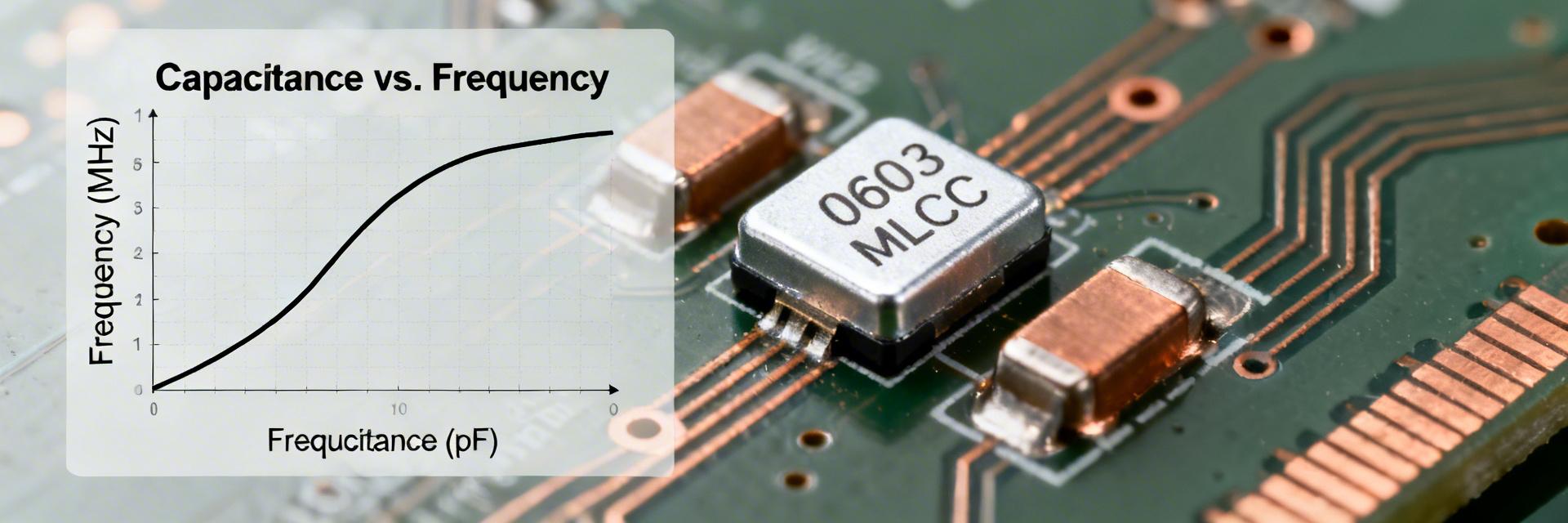
Point: 0603 MLCCs in the 10pF–100pF range are optimized for bypass, filtering, and coupling in space-constrained designs.
Evidence: Lab measurements confirm expected capacitance vs. frequency behavior and Self-Resonant Frequency (SRF) in this size class.
Explanation: Expect a compact footprint but account for lower absolute capacitance and pronounced DC-bias effects; ideal for decoupling supply rails.
Electrical Characteristics & Specifications
Key specifications include nominal capacitance, tolerance, rated DC voltage, C vs. DC-bias curves, temperature characteristics, dissipation factor (DF), and insulation resistance. Each metric directly influences circuit filtering effectiveness and long-term stability.
| Parameter | Datasheet (typ/lim) | Measured Performance | Visualized Tolerance |
|---|---|---|---|
| Nominal Capacitance | 56 pF ±5% | ~54–58 pF |
|
| Rated DC Voltage | 50 V | N/A (Static) |
|
| C vs DC Bias | Specified Curve | 20–40% Drop @ Rated V |
|
| DF / ESR | DF < 0.02 | Matches Class Limits |
|
Operating Limits & Derating Guidance
Conservative derating of voltage and attention to temperature limits significantly improve long-term reliability. We recommend operating below 50–70% of the rated DC voltage for high-reliability applications and documenting expected capacitance shifts due to temperature variations.
Lab Test Methodology
Our test suite captures C vs. frequency, C vs. DC bias, and ESR/DF across the spectrum. We utilize sample sizes of 20–50 parts to ensure statistical relevance, documenting median values and deviations to inform real-world design margins.
Data Interpretation
Observed behaviors include capacitance reduction under bias and ESR spikes at resonance. Flag any results where capacitance loss exceeds design allowances or where significant post-reflow shifts occur; these may require extended aging tests.
Reliability & Qualification Checklist
Common Failure Modes
- • Mechanical cracking from PCB flexure.
- • Dielectric breakdown under overvoltage.
- • Solder-joint fatigue after thermal cycling.
Qualification Requirements
- • Temperature/Humidity Bias (THB) testing.
- • Solderability and reflow survivability.
- • Long-term DC-bias aging protocols.
PCB Implementation & Procurement
Assembly Best Practices
Utilize conservative land patterns and controlled solder paste apertures to mitigate cracking risks. Avoid "via-in-pad" designs near critical capacitors and strictly control reflow ramp rates to prevent thermal shock.
Procurement & BOM Management
Lock critical parameters: package size, nominal capacitance, tolerance, and dielectric class. When sourcing alternatives, ensure the C vs. bias curves match the original specification to maintain system-level performance.

