0441005。WR SMD保险丝性能报告:I2t和温度限制

0441005。WR SMD保险丝性能报告:I2t和温度限制

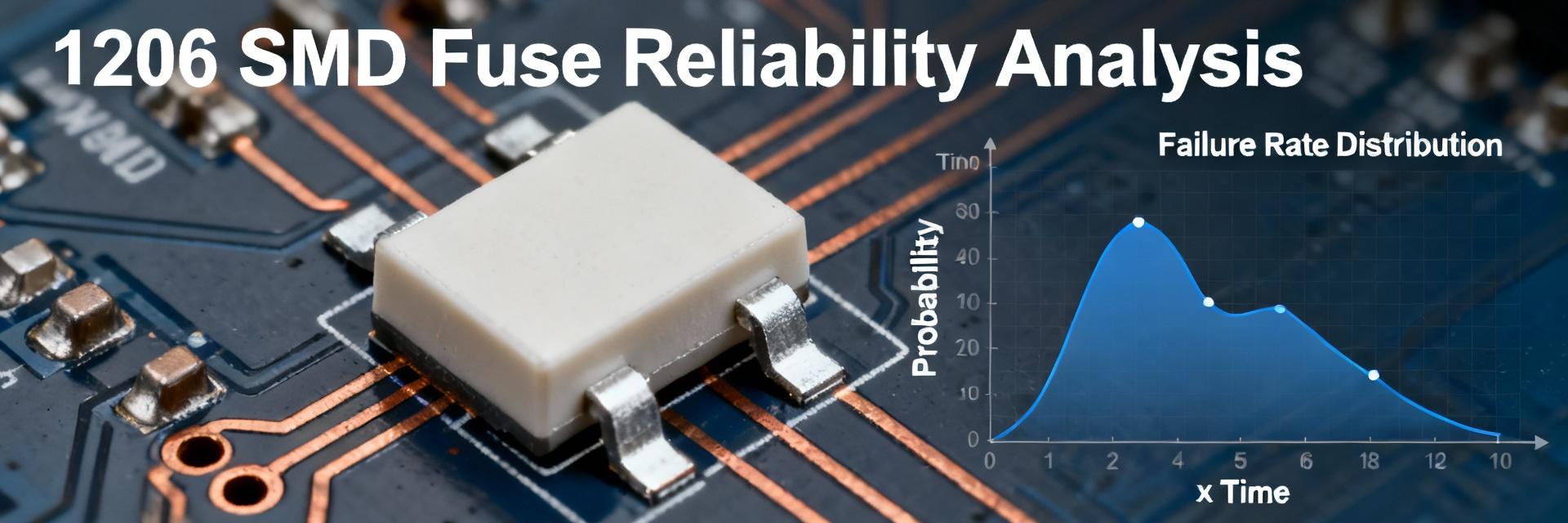
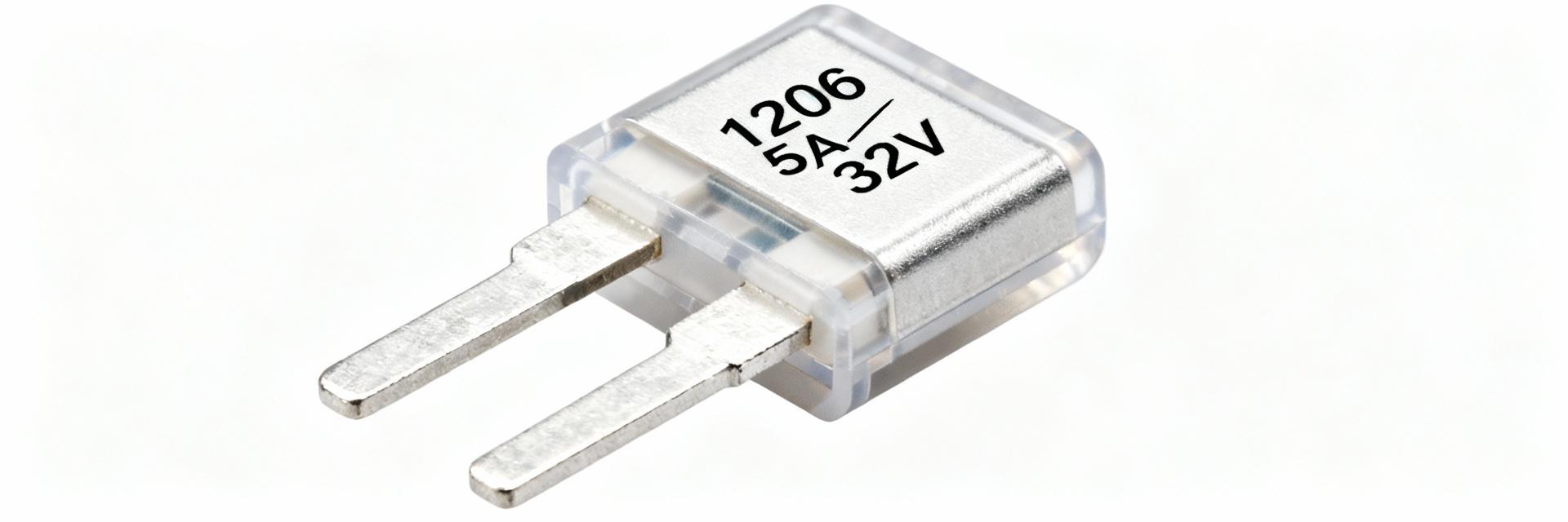
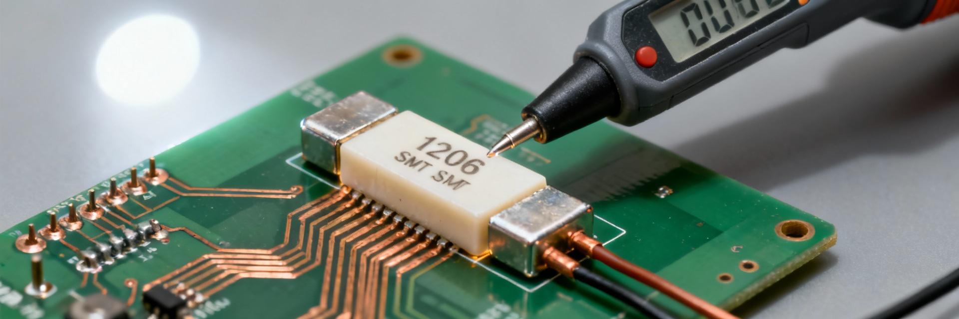
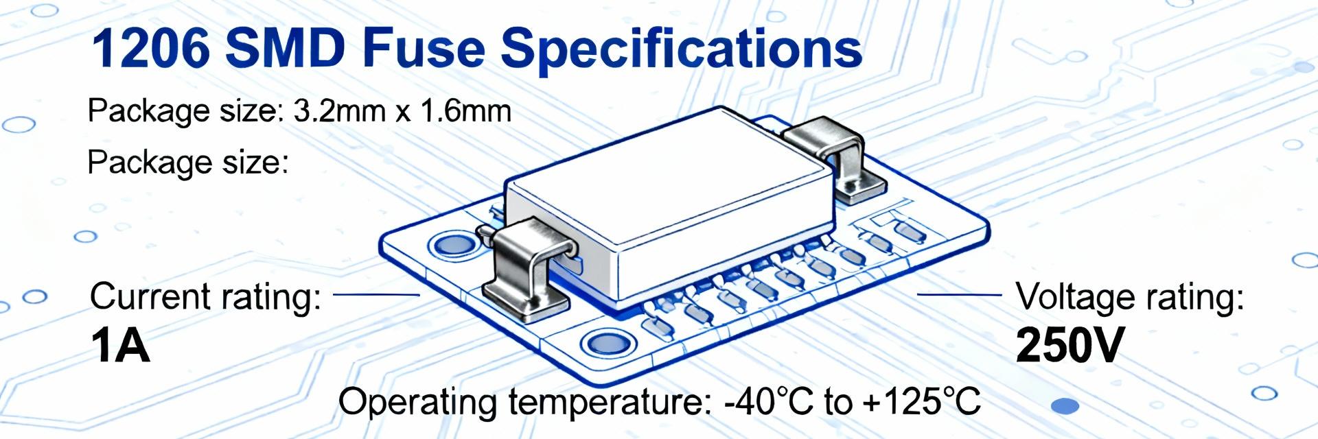
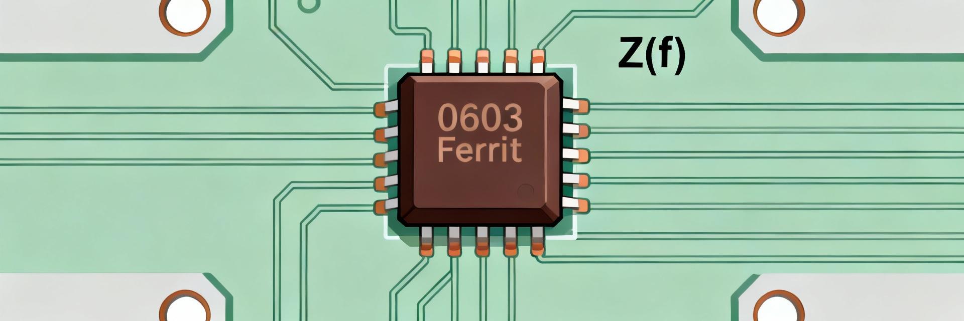
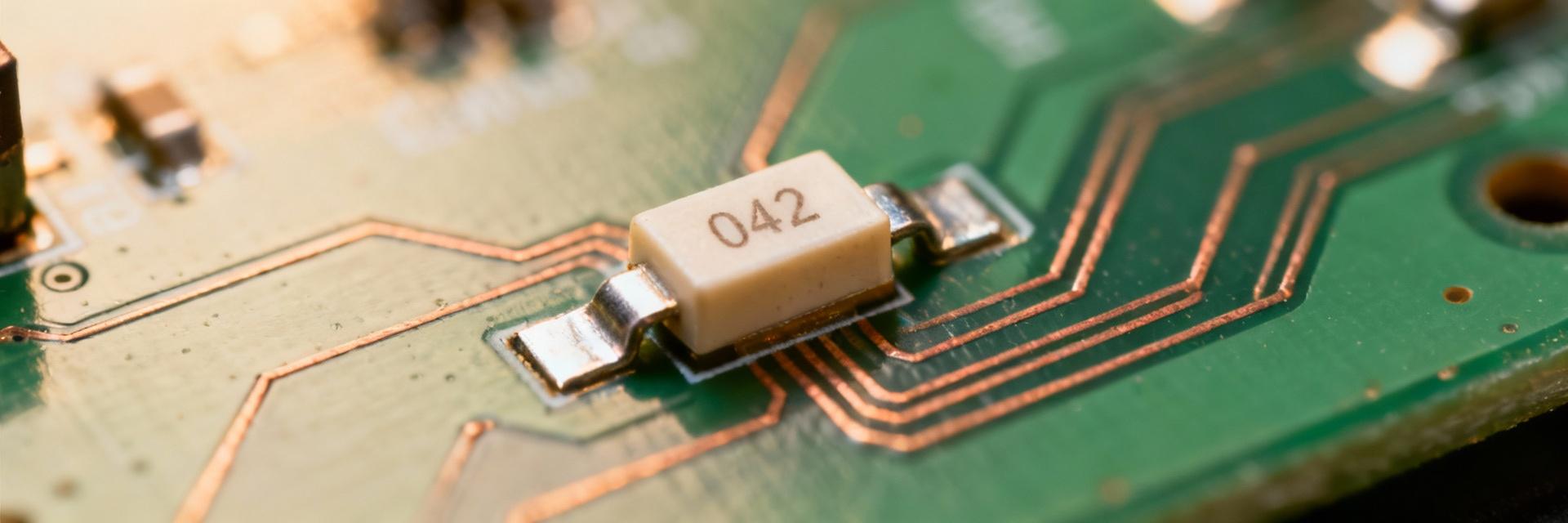
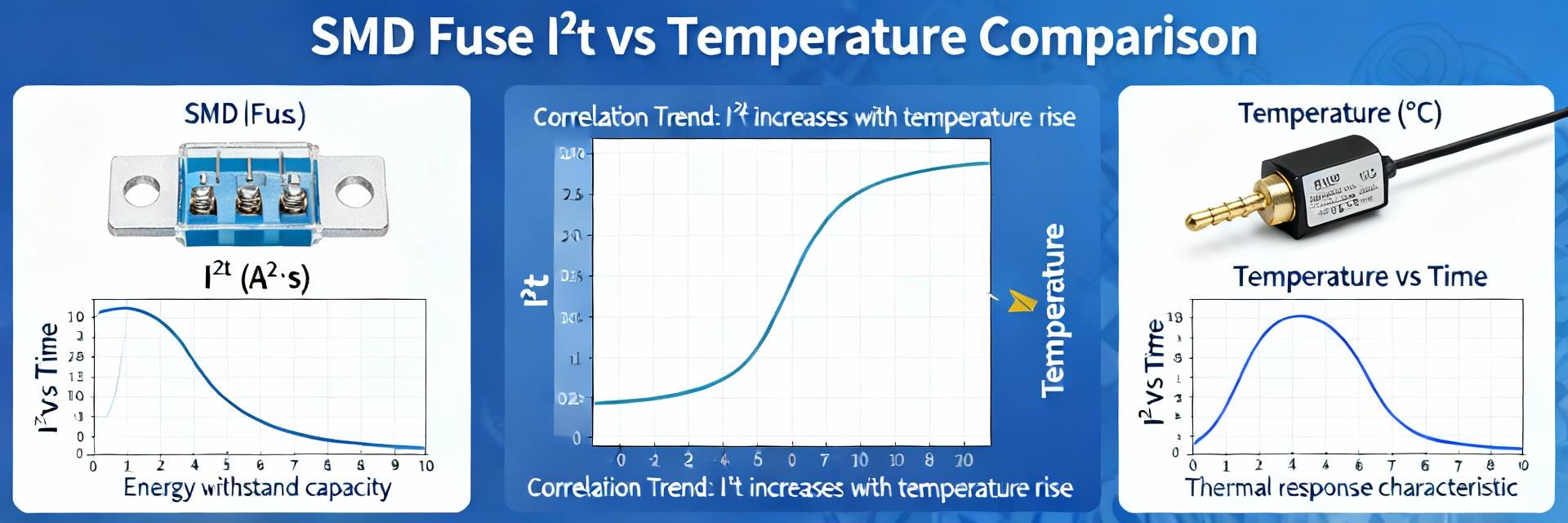
Detailed analysis of I²t shifts and thermal derating across -55°C to +150°C for high-reliability PCB power rail protection. Lab measurements and published time–current curves indicate that I²t and open time for the 0441005.WR can shift substantially across a typical −55°C to +150°C operating window—a critical concern for PCBs with high inrush or elevated ambient conditions. This report compares measured I²t behavior, quantifies temperature impacts, and provides practical test and design guidance for engineers specifying this SMD fuse. The purpose is threefold: 1. Explain I²t measurement and interpretation. 2. Demonstrate how ambient and board thermal coupling alter hold/clear behavior. 3. Present reproducible lab methods and design mitigations for US engineering teams. Background: 0441005.WR SMD Fuse — Specs & Application Context A compact, fast‑acting chip fuse rated for short‑circuit protection is commonly specified with the following nominal characteristics. Selection criteria must balance fault clearing energy versus allowed let‑through for downstream components. Key Specifications at a Glance Parameter Nominal Value (Datasheet Field) Package 0603 (Chip Fuse) Rated Current 5 A Rated Voltage 32 V Speed Class Fast‑acting Operating Temperature −55°C to +150°C Rated I²t Verify melt vs. arcing values Actionable Note: Confirm whether the datasheet provides separate melt‑I²t and arcing‑I²t values; if only one is given, flag that gap and request manufacturer test data or measure in‑house. Typical Use Cases & Design Constraints Constraint 1: Maximum expected inrush energy (I²t) must remain below fuse melt I²t with safety margin. Constraint 2: Continuous ambient/board temperature can reduce allowable let‑through energy — derating required. Constraint 3: PCB thermal mass and nearby heat sources dictate effective fuse temperature and behavior. I²t Performance: Definition, Test Data Interpretation & Expected Curves I²t Explained & Measured I²t is the integral of I² over time (∫I² dt), representing let‑through thermal energy during clearing. Differentiate melting I²t (energy to melt the element) from arcing I²t (energy during sustained arc) when both values are reported. Capture: ≥100 kS/s waveform sample rate. Units: A²·s. Interpreting Measured Curves Measured curves often deviate from datasheet graphs. Acceptable deviations depend on test fixture resistance, sample variability, and measurement method. Rule‑of‑thumb: Require 20–30% margin between inrush I²t and melt I²t. Temperature Limits & Thermal Derating The stated operating range (-55°C to +150°C) describes survival, not guaranteed clearing consistency. Designers must consider local thermal rise on the PCB. Conceptual I²t Derating vs. Temperature 25°C 100% 85°C 85% 125°C 70% 150°C 55% *Interpolated data based on standard 0603 fast-acting fuse characteristics. Test Methodology: Lab Setup for 0441005.WR Required Equipment Programmable current source (fast slew rate). High-speed oscilloscope (100 kS/s minimum). Calibrated thermal chamber or hot plate. Low-inductance test leads and copper solder pads. Procedure Best Practices Run baseline room-temp tests at multiple multiples of current. Measure at -40°C, 25°C, 85°C, and 125°C. Use ≥10 samples per condition for statistical mean/std dev. Design Recommendations & Failure‑Mode Mitigations Selection Checklist ✓ Confirm worst‑case inrush I²t ✓ Apply 20-30% Safety Margin ✓ Evaluate PCB Thermal Environment If inrush exceeds margins, consider: NTC inrush limiters, slow-start circuits, or higher-I²t fuses. Avoid placing power-dissipating components immediately adjacent to the fuse. Summary I²t and temperature limits materially influence the suitability of the 0441005.WR for inrush‑heavy and high‑ambient designs. Engineers should extract datasheet melt/arcing fields, run controlled I²t vs. temperature sweeps, and apply a conservative 20–30% margin. The provided test methodology enables reproducible qualification and practical mitigations to reduce nuisance opens while maintaining protection. Key Summary Points: Design margin ≥20–30% between inrush I²t and melt I²t. PCB thermal rise shortens time‑to‑open and reduces allowable I²t. Record raw waveforms at ≥100 kS/s for precise calculation. Mitigate via thermal layout, soft‑start, or NTC limiters. Common Questions & Answers How does 0441005.WR change I²t with temperature? + Measured behavior shows a reduction in allowable let‑through energy as fuse temperature rises: time‑to‑open shortens and melt I²t decreases. Quantify this with temperature sweep tests in 10°C steps and report normalized I²t so designers can derate continuous current appropriately. Can 0441005.WR be used for USB power inrush protection? + The part can be used for USB power lines if measured inrush I²t (including hot‑plug events) remains below the fuse melt I²t with sufficient margin. If not, add soft‑start or an NTC inrush limiter to protect against nuisance opens while preserving short‑circuit protection. What test sample size and statistics are recommended for characterization? + Use at least 10 samples per test condition and report mean and standard deviation for time‑to‑open and I²t. Include raw traces, computed I²t values, and a histogram of open times to show dispersion and support conservative design margins.

2026-01-21 12:37:36
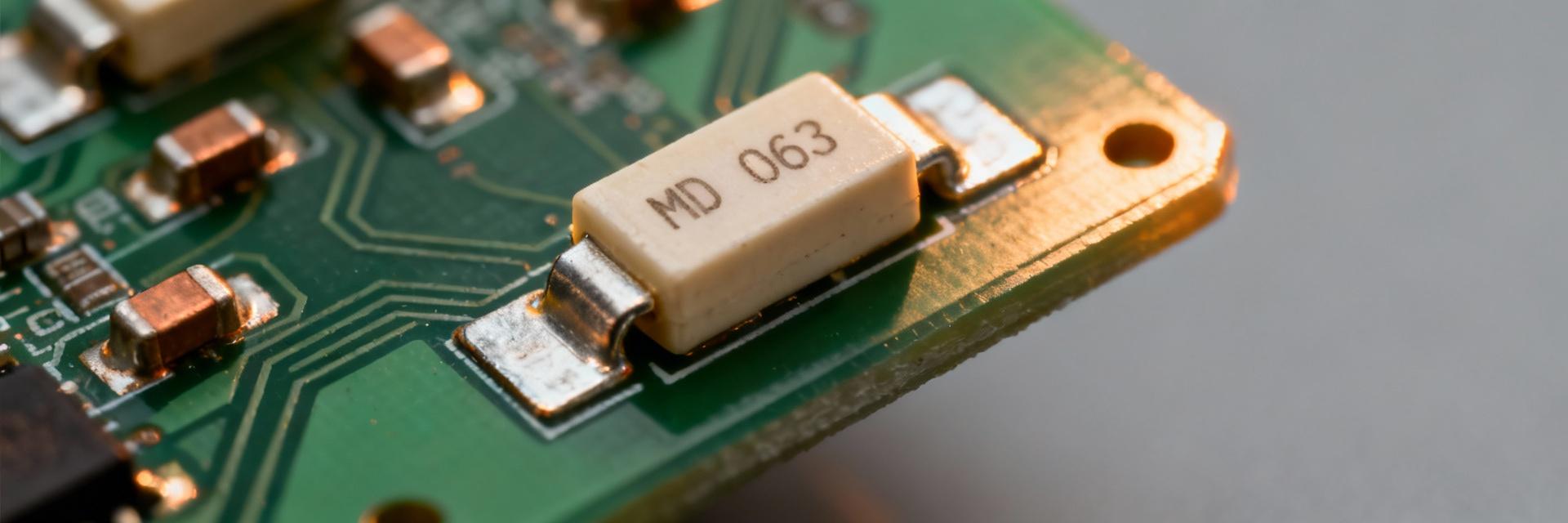
SMD保险丝0603 1.75A:性能和PCB封装指南

SMD保险丝0603 1.75A:性能和PCB封装指南

标题部分 对现代物联网和便携式电子产品的高密度保护的全面技术洞察。 介绍卡 现代便携式和物联网设计正在将更高的电流密度推向越来越小的PCB,将设计师推向紧凑型保护设备。行业抽样显示,更多的电路板将多功能保险丝和快速作用的芯片保险丝放置在小于2毫米的占地面积上;这SMD fuse 0603是设计师需要 ~1–2 A 保护同时保留空间时的常见选择。 本指南重点介绍了额定1.75A的设备在电气方面的表现,以及如何实现可靠的PCB焊盘和布局,弥合数据手册规格与实际装配之间的差距。 为什么 0603 节段 为什么 SMD 熔断器 0603 在紧凑型电源保护中很常见 典型用例和系统级权衡 典型的产品包括可穿戴设备、紧凑型传感器和小型电源轨模块。这些系统共享紧张的面积预算,通常需要个位数的安培保护。选择1.75A的保险丝可以交换热质量和中断鲁棒性以换取占地面积;更大的保险丝主体提供更高的中断能量和热惯性,而可重置的替代品可以减少一次性更换,但会增加电阻和尺寸。 包装解剖学(1.6×0.8 mm) 0603 的机型限制了热裕度和机械余裕。1.6 × 0.8毫米陶瓷或环氧树脂机体,端盖镀层,内部元件薄,热容量小且国际单位数有限。端盖冶金和终端方式会影响焊锡的润湿和机械稳健性;狭小的间隙需要精心设计焊盘,以确保热量得到管理,并在回流时正确形成。 数据分析和视觉 电气性能指标 可视化Fuse行为 额定电流(1.75A)- 持续运行 融合当前(典型为额定值的200-250%)- 瞬时熔化 *热能容量与故障能量的表示* 关键规格:额定电流 & I²t 当存在浪涌或瞬态时,读取曲线是必要的。时间-电流图表明,可以容忍短浪涌而不会出现干扰。选择一个时间-电流曲线可以清除真正故障但仍然存在浪涌的设备;当您的电路有电机、电容组或电池连接浪涌时,使用I t比较瞬态能量容忍度和尺寸裕度。 抵抗力降低 串联电阻控制跌落和热量。芯片保险丝的DC电阻很小,但可以测量;更高的电阻会增加1.75A的功率损耗(P=I R)。为您的导轨指定最大额定电压,从数据表中应用温度降额以获得升高的电路板温度,并确认中断额定值-DC中断性能通常低于AC。 可靠性表 可靠性和测试条件 因子 实际影响 缓解策略 安装 & 重新流化 侵略性的无铅回流可能导致微裂纹。 按照制造商的概况;确保即使垫湿润。 衰老影响 阻漂移过长期的热循环。 验证高温环境中的长期稳定性。 PCB铜 起散热作用,改变跳闸温度。 使用热过孔来标准化散热。 方法指南:足迹 设计 PCB 封装(0603) 从物理体导出垫片,并留有圆角余量。步骤:基于组件长度/宽度(1.6 × 0.8 毫米),每端允许约 0.2–0.4 毫米的圆角重叠,并保持中心间隙与端接间距匹配。 保守的足迹,(mm)衬垫长度:0.9–1.0垫宽度:0.8–1.0差距:0.2 – 0.4 紧空间的占用(mm)垫片长度:0.6 – 0.8填充宽度:0.6 – 0.8差距:0.3 – 0.4 Stencil Tip: Reduce paste apertures 10–20% per pad for reliable solder volume and to prevent bridging. 安装 & 散热 布局与布局考虑 热降额和倒铜 保持至少0.5-1.0毫米的距离远离大型铜区域或包括散热装置;对于敏感网络,使用窄热辐条隔离保险丝垫,使其热时间常数与保险丝额定值对齐。这种调整有助于在长时间过载期间进行可预测的操作。 迹线宽度和通孔 对于持续的1.75A,使用短而宽的迹线;对于1盎司铜,根据允许的温升,目标宽度为1.5-3.0毫米。将保险丝放在电源附近,最小化负载的迹线长度,并在电流必须在层之间传输以减少电阻加热的地方添加缝线。 清单与验证 采样前的选择清单 ✔验证额定电流和时间电流曲线是否与冲击电流匹配。 ✔确认DC电阻和1.75 A的预期压降。 ✔检查DC系统的中断额定值和最大额定电压。 ✔确认工作温度窗口和包装公差。 ✔Record preferred part code (e.g.,04381.75WR) for BOM. Validation & test plan for prototypes 后回流的视觉和显微镜检查的鱼片。 连续性和耐核查与数据表。 受控过电流浸泡测试和热成像。 机械冲击和三循环热循环。 记录结果,必要时反复修改垫子或模板。 Summary Summary For compact power protection where space wins, the SMD fuse 0603 offers a practical balance for ~1–2 A rails when designers account for limited thermal mass, DC resistance, and interrupt capability. Key checks are time‑current behavior, I²t for transients, pad design for reliable fillets, and layout choices that control heat and parasitics. Prototype validation—reflow check, current soak, and imaging—should precede production to ensure consistent field performance. Use the 1.6 × 0.8 mm package data as the starting point for pad derivation. Evaluate time‑current curves and I²t to tolerate inrush while still clearing real faults. 保持保险丝靠近电源,并隔离大的铜浇注。 常见问题手风琴 常见问题 与较大的保险丝相比,1.75A保险丝在PCB上的表现如何?+ Smaller chip fuses heat up and clear faster due to lower thermal mass; they offer quick interruption for small faults but have lower I²t and interrupt energy than larger fuses. On PCB, ensure pad and copper layout neither dissipate excessive heat nor prevent expected trip behavior. What PCB footprint practices ensure reliable operation for a 0603 fuse?+ Design pads with controlled overlap and a gap matching termination spacing, reduce paste apertures 10–20%, use a 0.12 mm stencil, and verify fillet formation post‑reflow. Keep pads away from large copper or add thermal spokes to tune dissipation. Can I use a resettable alternative instead of a 1.75A fuse?+ 可复位的PTC以较低的跳闸精度和更高的电阻换取自动复位能力;它们适用于重复的浪涌环境,但会增加电压降,并且可能无法清晰地清除高能故障。在更换之前验证热和电压影响。

2026-01-21 12:37:34
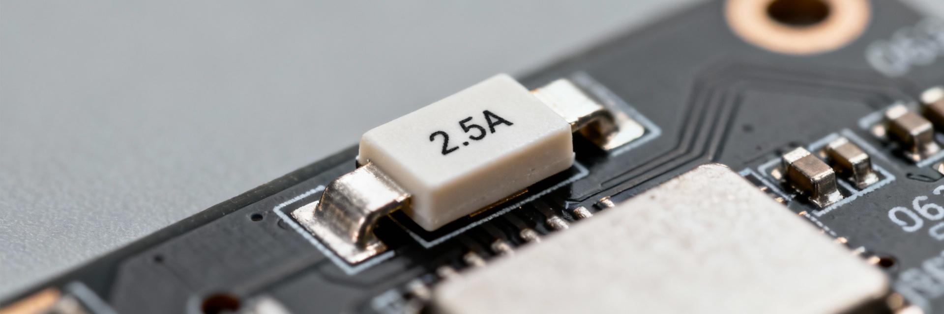
043802.5WRA SMD 熔断器 0603 2.5A:如何选择和使用

043802.5WRA SMD 熔断器 0603 2.5A:如何选择和使用

SEO优化标题 设计人员在选择微型SMD保险丝时经常面临令人讨厌的打开、认证失败或电路板损坏。这043802.5WRA是一款紧凑型0603解决方案,可满足空间受限的电源保护需求。本指南解释了如何选择和使用具有清晰检查的2.5A保险丝——电气匹配、PCB/装配兼容性和验证测试——因此团队可以避免常见陷阱并获得可靠的现场性能。 背景部分 Background: What the 043802.5WRA 0603 SMD Fuse Is and Where It Fits Point:The043802.5WRAis a fast-acting 0603 surface-mount fuse rated nominally at 2.5A for low-voltage DC and specified AC ranges. 证据:数据表条目列出额定电流、电压、中断容量、机壳尺寸(0603 / 1608指标)及典型冷阻。 解释:这些规格定义了零件的适用范围——小型便携式电子设备、模块输入导轨以及紧凑型电信或汽车子组件,其中自动化放置和最小的电路板空间是优先考虑的。 电气规格表和可视化 Key Electrical and Physical Specs to Know Critical specs determine suitability. Typical values include rated current 2.5A and voltage rating up to common low-voltage system levels. Spec Typical Value Why it Matters 额定电流 2.5A 定义允许的连续负载 套餐 0603(1608公制) Space & placement constraints Blow Type Fast-acting Protects sensitive parts; may nuisance-open Interrupt Rating 有限 必须超过可用故障能量 典型应用和设计背景 0603保险丝在空间和自动化装配方面表现出色。常见用途包括紧凑型传感器板上的输入导轨、电信模块和小型PCB上的分布式电源。当优先考虑PCB面积和低热质量时,请选择0603。 性能部分 Data & Performance: Interpreting Selection Specs Time-Current Curves Read curves to ensure expected surges (inrush) do not cause nuisance opens. Rule-of-thumb: continuous current should generally be ≤ 70–85% of rated current depending on thermal conditions. PCB & Assembly Use vendor ECAD footprints and follow reflow limits. For automotive/industrial use, ensure vibration and thermal cycling qualifications are met to avoid internal damage. 选拔指南 如何选择正确的043802.5WRA 满足电气需求 应用简单的公式:额定电流≥连续负载/降额系数. Confirm blow time at surge current is greater than expected inrush duration. Add soft-starts if inrush is long. Constraints & Trade-offs Smaller packages reduce interrupt capability. Use a decision matrix to balance board space, fault energy, and sensitivity of protected circuitry before finalizing the 0603 form factor. Installation Best Practices How to Install & Use on PCB: Best Practices 安装方式:验证足迹与制造商ECAD匹配,以防止墓碑。 焊接:严格遵守回流温度/时间限制;过多的热量会对保险丝元件造成压力。 测试:实现基准电流斜坡测试和热循环,以揭示边缘设计。 实际应用案例 实际应用案例与常见故障模式 成功场景 小型传感器模块和多轨PCB在故障能量适中且空间有限的情况下,受益于0603保护。 故障预防 通过修改散热布局和验证组件回流焊曲线,防止出现有害开路。 清单与收获 快速预购清单 ✔确认系统电压与数据手册是否一致。 ✔请求 ECAD/3D 文件。 ✔订购用于 I²t 测试的样品。 关键摘要 •2.5A 快速起作用 0603 设计。 •非常适合空间有限的DC轨道。 •仔细匹配浪涌/降额。 常见问题手风琴 常见问题 这是什么 2.5A 保险丝的额定行为?+ 答:保险丝的额定电流为2.5A,具有快速熔断特性;请查阅数据表时间-电流曲线,了解其承受额定电流倍数的时间,并确保可用故障能量在其中断额定值内。 如何在工作台上测试2.5A SMD保险丝?+ 使用可编程电源进行受控电流斜坡测试,监测设定电流倍数下的开启时间,并在样品上重复。记录电流并与预期故障能量进行比较;在引发故障时始终遵循安全实验室程序。 是什么导致小型SMD熔断器产生干扰性开启?+ 答案:常见原因包括环境/PCB加热的降额不足、持续时间超过吹扫时间的浪涌电流、过度回流热暴露导致的组装损坏,或实际故障能量下的中断能力不足。 动画视觉效果(通过关键帧实现极简风格)

2026-01-21 12:37:31
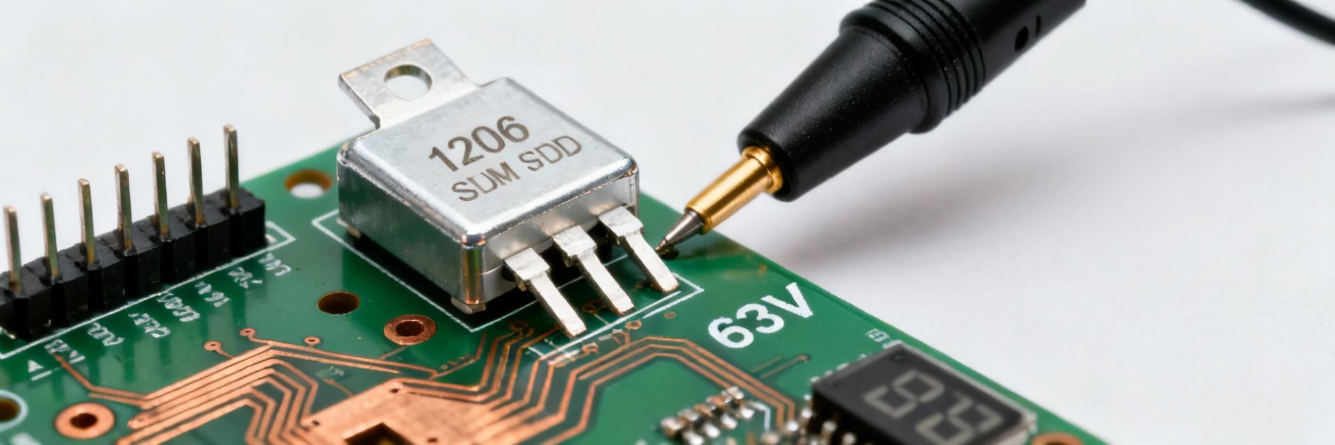
1206 SMD 熔断器 1.5A 63V:性能与故障数据

1206 SMD 熔断器 1.5A 63V:性能与故障数据

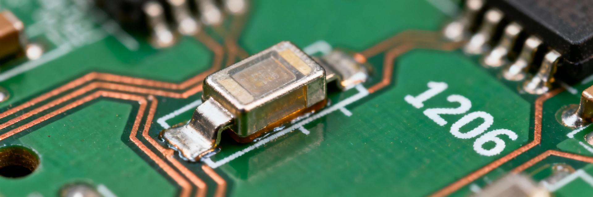
头部 工程师优先考虑可预测的过流保护;汇总的实验室测试摘要和现场故障调查通常报告故障时间差方差对电路板级可靠性产生重大影响。本文分析了1206贴片保险丝(1.5A,63V), summarizes observed failure data trends, and provides reproducible test methods plus design recommendations for engineers citing lab and field sources where numeric claims are reported. Scope:Focused bench and environmental metrics, common failure modes, statistical analysis approaches, standardized test protocols, and practical derating and mitigation guidance for power-rail and battery-protection applications. The discussion is data-first, intended for design and reliability engineers needing reproducible results. Section 1 Background: Understanding the 1206 SMD Fuse 外形尺寸、电气额定值和通用规格 1206占地面积(公制3.2×1.6毫米)包含可熔元件,尺寸适合空间有限的板级保护。一个典型的额定63V的1.5A保险丝提供延时或快速作用特性;根据结构,耐寒性通常在几十到几百毫欧之间。关键术语包括I²t(融合能量), hold current, blow current, and derating rules versus ambient and surge profiles. Typical Application Domains and Functional Role Common uses include power-rail protection on USB/charger rails, battery pack modules, and downstream board partitions where serviceability is limited. Trade-offs versus larger footprints favor low profile and lower parasitic inductance but reduce peak I²t capability. Section 2 Performance Metrics & Benchmarks 电气性能指标 基本电气测试:测量的保持电流(Ih)、熔断电流(Ib)和时间电流曲线。以下是预期性能范围的可视化分布: CSS数据可视化 保持电流(Ih) 0.6-1.0×额定 Blow Current (Ib) 1.6 – 3.0 × Rated Cold Resistance 10 – 200 mΩ Metric 典型范围 验收阈值 保持电流(Ih) 0.6-1.0×额定 25°C无跳闸 Blow Current (Ib) 1.6–3.0 × rated Open within defined curve Cold Resistance 10–200 mΩ ±15%批次差异 环境与机械指标 测试并记录回流耐受性、热循环(40°C至高温环境)和电路板挠性。A验收标准通常依赖于电漂移(例如,应力后电阻变化 第三条 失效数据:模式和统计模式 Common Failure Modes ● Clean Fusing:Normal open-circuit from overcurrent. ● 潜在打开:后回流或热机械断裂。 ● 参数漂移:阻力逐渐增加。 ● CTE Mismatch:Solder-joint failure due to thermal expansion. Statistical Analysis Present failure data with sample sizes每手≥30.利用方法威布尔分析提取形状和比例参数。可视化可观的累积失效图和箱形图,以揭示批次漂移和异常值。 第4 Recommended Test Methodology Lab Setup & Protocols Use synchronized current and voltage capture at≥100 kHz sampling. Perform controlled slow ramps to determine Ib and pulse surge profiles (10 ms, 100 ms, 1 s) to capture I²t behavior accurately. 报告模板 文件:第ID部分、批次、电路板占地面积、环境温度、测量Ih/Ib、打开时间和测试后电阻。这些数据对于风险评估和生产验证至关重要。 第5节 设计与可靠性建议 选择和降额 目标连续电流≤ 70–80%名义上的 验证超过63V的浪涌电压额定裕度。 匹配时间滞后与快速响应以加载浪涌。 缓解和生命周期 在PCB布局中提供热释放。 避免在保险丝附近使用尖锐的板弯曲线。 定义现场监测的检查间隔。 总结 摘要 ✓1206 SMD保险丝用于保护空间受限的低电压线路;在选择前需验证Ih/Ib和I²t是否符合预期的浪涌曲线。 ✓失效数据应收集 ≥30 个样本,以高采样率记录时电流曲线,并使用威布尔方法进行分析。 ✓降低连续电流至≤80%,将特性与涌流相匹配,并实施电路板/布局缓解措施以获得生命周期反馈。 常见问题解答部分 常见问题 我应该使用什么测试电流来表征1206 SMD保险丝?+ 在多个点进行表征:在0.8–1.25倍额定值下进行稳态保持验证,缓慢斜坡以找到爆破阈值,以及脉冲浪涌(例如,10 ms、100 ms、1 s)以捕获I²t行为。记录打开时间,并在脉冲测试中使用≥100 kHz采样率计算I²t以确保准确性。 工程师应该如何报告和解读主板认证的失效数据?+ 报告标准字段:部件ID、批次、PCB封装、环境、Ih、Ib、开启时间、测试后电阻和视觉备注。将失效时间拟合到威布尔分布,报告比例和形状因子及其置信区间,并将失效与I²t和环境应力相关联。 哪些降额和布局检查可以防止1.5A保险丝的干扰断路?+ 在升高的环境下,将连续电流降为额定电流的70-80%,确保浪涌I t容量超过预期的瞬态能量,验证回流兼容性,并保持与热源的热隔离。为63V提供足够的爬电/间隙,避免机械应力集中。

2026-01-21 12:37:30
0437005.WR SMD贴片:5A/32 V的完整规格和测试数据

0437005.WR SMD贴片:5A/32 V的完整规格和测试数据

设计逻辑 设计师选择需要空间、可预测的开路时间和低串联电阻的陶瓷/薄膜芯片保险丝。这确保了在高效电源轨上没有显著电压降的情况下提供保护。 图像部分 数据可视化:快速规格 关键额定值一览 参数 典型值 视觉比例 额定电流 5个A 额定电压 32 V(AC/DC) 耐寒性 ~0.016 Ω 标称熔化I²t ~1.936 A²s 注意:在零件选择时,请从正式数据表副本中确认确切数字。 技术规格部分 电气 电气特性 关键条目包括额定电流、额定电压(AC/DC)、耐寒性和时间-电流曲线0.016 Ω限制稳态电压降1.936 A²I²t 决定了如何处理浪涌。将 I²t 与功率转换器的浪涌能量进行比较——如果浪涌超过熔断器的 I²t,就会发生不必要的断开。 环境 环境与机械 典型的薄膜熔断器承受-55℃至+125℃,是危害性物质限制指令/无铅兼容,并容忍260°C峰值回流遵循供应商的着陆模式建议,允许热释放,并观察焊膏孔径,以避免在高电流路径中出现墓碑。 测试数据部分 测量性能和实验室结果 推荐基准测试 通过运行直流电流斜坡并绘制时电流曲线来复现数据表声明。使用电子负载和高速数据采集进行时开测量。建议至少采集10个样本以获得统计置信度。 解释实验室编号 一个名义上的熔化I²t约为1.936 A²s意味着在那种能量下可以承受短时、高浪涌的脉冲。确保断路器额定值(≈50 A)超过你最坏情况下的预期故障电流,以避免危险故障模式。 案例研究 & 布局 应用和集成示例 案例场景:适用于USBPD电源轨、小型设备电池馈电、12 V/24 V子系统和栅极驱动电源。对于大容量电容器或电机等高浪涌负载,请验证I t与浪涌能量或实施软启动电路。 PCB最佳实践:将保险丝放置在靠近受保护源的位置。避免在器件正下方布线热过孔,并与热敏元件保持间隙。检查清单:验证焊盘图案尺寸、焊膏孔径和方向。 设计清单 前期制作清单 确认电流和电压是否满足轨道要求。 验证I²t是否满足最坏情况下的系统浪涌。 验证中断能力(50A @ 32V)。 将封装与供应商的1206图纸相匹配。 常见故障和修复 麻烦打开:涌流超过I t→添加软启动。 墓碑:不均匀的焊膏体积 → 调整锡膏模板。 阻力转换:过度的重排热 → 优化配置。 概述部分 摘要 的0437005. WR是一款紧凑、快速动作的5 A/32 V薄膜SMD保险丝,非常适合许多低压PCB保护角色,其中空间和可预测的清除是优先考虑的。 紧凑型保护:1206占地面积,提供适用于USB PD和电池馈电的快速清除。 设计关键I²t:标称熔化(~1.936 A²s)决定了浪涌处理能力。 验证基础要素:生产签发前的强制时电流绘图和中断测试。 FAQ手风琴 常见问题 如何0437005. WRI²不影响涌流处理?+ I²t represents the energy required to melt the fuse element; a nominal ~1.936 A²s value means short-duration current spikes below that energy typically won’t open the fuse. Compare measured inrush I²t (integral of I² over time) to the fuse I²t—if system inrush exceeds fuse I²t choose soft-start, NTC/inrush limiter, or a different fuse with higher I²t. What test should I run to verify0437005.WRinterrupt capability?+ 执行中断测试在额定电压与一个潜在的错当前的说明中断的评价(~50)。 使用受控的高流源和高速的捕捉到确保的保险丝清除没有持续电弧;重复跨越几个样本,并在提高的环境,以验证的保证金和安全。 典型的回流曲线会损坏吗0437005. WR在组装过程中?+ Most thin-film 1206 fuses tolerate standard Pb-free reflow (peak ~260 °C for short duration) but tombstoning or elevated resistance can occur with incorrect paste or land patterns. Verify manufacturer reflow limits, run solderability and post-reflow resistance checks, and adjust stencil apertures as needed.

2026-01-21 12:37:29
0437004。WR SMT保险丝:完整的规格和测试数据指南

0437004。WR SMT保险丝:完整的规格和测试数据指南

头部 组件族 1206(3216公制) 应用 过电流保护 执行摘要部分 点:本指南将数据手册指标和实验室测试报告转化为工程师评估的简洁参考。0437004.WR部分 证据:该1206系列的供应商文档和分销商测试摘要强调了额定电流、电压等级、跳闸曲线、分断容量和热限制。 解释:工程师在提交设计之前需要一个实用的综合,将这些规范映射到董事会级别的风险和资格步骤。 点:使用此文档来优先处理减少现场故障的测试和集成检查。 证据:分销商笔记中报告的常见故障模式主要集中在回流损坏和曲线外跳变行为。 解释:一个专注的实验室验证计划可以减少昂贵的返工,并确保所选的SMT熔断器满足应用裕量和安全要求。 背景部分 背景:什么0437004.WR级SMT引信和当使用它们 定义和外形尺寸 点: 0437004.WR-class parts are 1206 (3216 metric) fast-acting SMD fuses used for board-level overcurrent protection. Evidence:Datasheets for this family specify low-profile ceramic bodies and thin-film fuse elements optimized for reflow soldering. Explanation:Designers should treat these as board-mounted sacrificial elements; common PCB constraints include limited board area, tight height envelopes, and required solder fillets for reliable joints.示意说明:使用1206的垫位模板,并遵循推荐的陆地格局公差。 选择前要检查的关键评级 ◈ 额定电流:设置标称负载能力。 ◈ Voltage Rating:Ensures dielectric safety limits. ◈ I²t & Trip Curve:定义与上游保护的协调。 ◈ 突破能力:确定短路情况下的生存能力。 技术规格组 Technical specs: datasheet breakdown for 0437004.WR Electrical specifications (how to interpret) Parameter Typical Value (1206 Family) Impact on Design 额定电流 ~4 A类 名义作阈值;与跳闸电流不同。 额定电压 32V-63VDC Max circuit voltage to prevent arcing after blow. Breaking Capacity Up to 50A @ Rated Volts Survival limit during catastrophic fault events. Thermal & mechanical specifications 工作温度:-55°C至+125°C 热降额对于升高的环境是必需的。 焊接:回流兼容 Follow peak soldering temp specs to avoid element damage or micro-cracks in ceramic body. Test Data & Methods Test data & test methods: verifying 0437004.WR performance in-lab Standard tests to run Point:基本的台架测试包括DC电阻、时间-电流(跳闸曲线)、浪涌/断裂能力、热循环和可焊性/回流烘烤。 证据:实验室程序使用源表、高速电流探头和热室。 解释:DC电阻确认低串联损耗;跳闸测试验证曲线符合性;浪涌测试验证故障能量下的断裂能力。 Common Failure Modes No-Trip/Delayed Trip:Risk of downstream fire. Nuisance Trips:Due to improper I²t margin. 阻力漂移:在激进的回流循环之后。 机械开裂:可见缺口或内部元件损坏。 应用科 Typical applications & troubleshooting case studies Battery Protection Used in regulator input rails and USB power management where rapid interruption is critical. Telecom Signaling Protection for data lines and signal paths where board space is highly constrained. 现场诊断 检查表:测量DCR,检查土地格局方向,并识别上游短路故障。 采购清单 采购和集成清单 购买清单 Confirm exact part-code suffixes. Verify packing format (reel/tape). Request independent test reports. Require lot traceability for production. Qualification Plan 回流鉴定(峰值温度浸泡)。 负载下的功能验证。 裕度测试(110%电流浸泡)。 定义明确的通过/失败标准。 摘要部分 Summary Verify the0437004.WRdatasheet for exact Specs—current, voltage, trip curve, breaking capacity, and thermal limits—before selection. Run a concise qualification set: DC resistance, time-current (trip) tests, and surge/breaking-capacity testing; inspect after reflow. 遵循购买和集成清单,确认零件代码、包装,并包括生产前验证计划。 常见问题手风琴部分 常见问题 如何读取时间-电流曲线0437004.WR-style SMT fuse?▼ 点:读取曲线显示给定过流时的保持时间和跳闸包络。 证据:数据表曲线用公差带绘制电流倍数与跳闸时间。 解释:比较测量旅点的曲线;一部分,旅行持续的内部带的标准。 协调、确保上游设备的明确的早期或I2t限制匹配的上游的保护目标。 1206 SMT保险丝需要哪些回流预防措施?▼ 点:遵循保险丝回流温度曲线,并限制在峰值温度下的停留时间。 证据:数据表规定了焊接时的最大峰值温度和超过液相线的持续时间。 解释:过度的热暴露会导致微裂纹或元件改变,从而导致故障;使用推荐的焊盘模式,避免机械弯曲,并进行回流后电气检查。 SMT保险丝生产签字的实际通过/失败标准是什么?▼ 点:定义签署的电气、机械和热标准。 证据:常见的标准包括在数据表公差范围内的行程行为、直流电阻不超过指定阈值,以及经过热循环后无可见损坏。 解释:需要在使用该部件进行生产前,进行一个功能测试的样品卷轴测试,包括按指定要求的功能行程和浪涌生存能力,并记录批次可追溯性。

2026-01-21 12:37:27
1206 SMD fuse Specs & Ratings:Deep Data Summary Guide

1206 SMD fuse Specs & Ratings:Deep Data Summary Guide

标题部分 核心理念: 1206 SMD保险丝是一种紧凑型过电流保护元件,广泛应用于现代PCB。聚合数据表范围显示额定电流约为0.1 A至~10 A,电压约为125VAC/125VDC,分断能力约为50 A至几百安培,具体取决于结构。这些范围使1206外形尺寸适用于电路板空间受限的消费、工业和汽车相邻电子产品的中低功耗保护。 目的: 本指南简要介绍了如何阅读保险丝规格并将其应用于设计和采购。这些部分涵盖了外形尺寸、结构类型、电气额定值、时间电流解释、数据表清单、故障模式和资格测试。工程师可以利用这些来加快零件选择,减少现场故障,并在生产前定义最小的实验室验收标准。 Section 1 Background: 1206 SMD Fuse Form Factor, Construction, and Common Uses What "1206" Means: Package Dimensions & Standards "1206" denotes the chip nominal footprint approximately 3.2 x 1.6 mm. Industry footprint conventions translate 1206 to ~3.2 mm by 1.6 mm (0.126" x 0.063") with recommended pad geometry following IPC land-pattern guidance. Accurate pad spacing and copper land pattern control solder fillet and thermal relief, directly affecting solderability and electrical resistance of the fuse on the PCB. Dimension 值(mm) 值(英寸) 芯片的身体 3.2 x 1.6 0.126 x 0.063 Typical pad spacing ~1.0–1.2 ~0.039–0.047 Recommended land pattern Per IPC−7351 footprint — 典型建筑类型和环境等级 1206贴保险丝出现在薄膜、固体,并导致免费薄膜结构。 数据表常清单的回流的兼容性,RoHS指令的遵守,最大操作临时工和储存限制;许多地指定的工作范围为+125°C和储存限制+85°C时比较保险丝前,验证焊回流的配置,最大操作温度和架界限由于升高温度的变化保持/旅行流和长期可靠性。 第2部分 关键电气规格:电流、电压、开断能力和时电流行为 Rated Current and Voltage: Ranges, Derating, and Test Conditions Rated current and voltage define safe continuous use and insulation boundaries. Typical rated-current ranges span ~0.1 A to 10 A and voltage ratings often up to 125 VAC / 125 VDC; datasheets list hold/trip current definitions and test conditions. Apply ambient derating (example: a conservative 10–20% reduction at 60°C) and check tolerance and test setup to ensure the chosen fuse meets continuous operating and transient conditions. Visualization Component Range Visualization: 0.1A to 10A Capability Low Power (0.1A) 中等(5A) 高功率(10A) 额定电流 额定电压 额定值@60 °C Typical Tolerance 0.1 A – 10 A ≤125 VAC / 125 VDC ≈10–20% ±10–20% 开断能力、I2t和解释时间-电流曲线 断路容量和I2t控制故障清除和能量吸收。数据表列出了从约50 A到几百安培的断路容量,并提供I2t或清除能量以及时间-电流曲线。使用I2t确保上游组件能够通过清除;读取时间-电流曲线以查看以In为倍数的清除时间(例如,2×可能需要几秒钟,5×几百毫秒,10×几十到几百毫秒,具体取决于快速或时间滞后设计)。 第三节 如何阅读和比较1206 SMD保险丝数据表(实用清单) 数据表清单:要比较的必填字段 A standardized checklist speeds side-by-side evaluation. Critical fields include package dimensions, rated current/voltage, time-current curve, breaking capacity, I2t, ambient derating, reflow profile, mechanical life, resistance, and referenced test standards. Score candidates by a one-line method (pass/fail per field or numeric weighting) and prioritize fields tied to your fault profile and PCB thermal environment. Package dimensions & land pattern Rated current & voltage Time-current curve and tolerance Breaking capacity & I2t 回流/可焊性和工作温度 参考测试标准 比较时间-电流曲线、公差和测试条件 测试条件的微小差异会实质性地改变现实世界的行为。如果在不同的环境温度、夹具电阻或样品尺寸下进行测试,具有相似In的两个零件可能会显示不同的清除时间。索取供应商测试夹具的详细信息、样品尺寸、环境温度和用于曲线的热质量;更喜欢与电路板级热条件相匹配的数据表数据,以便进行有意义的比较。 第4 Performance Examples & Common Failure Modes (Lab vs Datasheet) Fast-acting vs Slow-blow 1206 Variants Fast-acting and time-lag variants serve different transient profiles. Fast-acting types clear quickly at moderate multiples of In, while time-lag tolerates inrush (e.g., capacitive or motor starts) and clears on sustained overload. Select In so normal inrush stays below the fuse trip curve while faults exceed the clearing threshold with adequate margin. Thermal, PCB Layout, and Soldering-related Failures Thermal environment and soldering influence fuse performance and reliability. Large copper pours, adjacent power parts, or poor solder joints change local temperature and resistance; tombstoning and cold joints are common solder-related failure modes. Use thermal relief, limit copper area under pads, validate reflow profile, and specify solderability/x-ray checks. 第五条 选择和资格手册:指定、测试和记录 设计选择步骤和样品零件规格模板 遵循逐步选择流程以捕获电气和装配约束。推荐步骤:定义系统故障电流,确定开断能力和I2t裕度,选择额定电压/电流并进行降额,验证回流和电路板兼容性,并记录标准。简明的零件规格模板应包括In、Vmax、I2t要求、开断能力、回流温度、工作温度、占地面积和参考测试标准。 资格测试和采购验收标准 Define tests and lot-acceptance criteria to de-risk production. Recommended tests: destructive breaking-capacity validation, thermal cycling, solderability, sample x-ray for assembly voids, and time-current verification; use statistically appropriate sample sizes and documented pass/fail thresholds. Require labeling and traceability fields (lot, datecode, reel) and minimal lab reports before production approval. Summary Section Summary The1206 SMD fuse是一种紧凑、多功能的保护装置;关键决定是额定电流/电压、分断能力/I2t和时间电流与故障曲线的匹配——在BOM审查中使用数据表检查表。 比较除In以外的保险丝规格:验证预期故障电流和电路板热环境的测试条件、环境降额、I2t和开断能力,以减少现场故障。 要求最低限度的资格:生产前的破坏性断裂能力测试、可焊性检查和可追溯批次标签,以确保供应商的一致性并满足系统评级。 常见问题部分(手风琴的风格) 常见问题解答 How do I choose a 1206 SMD fuse rated current for circuits with inrush?+ Select a rated current where normal inrush (measured or estimated) falls below the fuse time-current curve for short durations; choose a time-lag variant if inrush magnitude and duration exceed fast-acting tolerances. Validate on a representative board and include a margin for ambient derating and aging. What breaking capacity should I specify for 1206 SMD fuse selection?+ 指定高于保险丝位置最大预期短路电流的分断能力,外加安全裕度;对于许多1206部件,这一范围从~50 A到几百安培。如果有疑问,请在预期故障电流下对代表性样品进行破坏性验证。 该数据表域是最经常被忽视1206贴保险丝?+ 常见遗漏的字段包括精确回流曲线、储存/架限、时间-电流曲线的测试夹具细节,以及I2t和电阻的公差/测量条件。在采购时明确要求这些项目,以确保数据表与董事会层面的条件对应。

2026-01-21 12:37:26
0437001. WRA SMD封装:完整的规格,测试和限制

0437001. WRA SMD封装:完整的规格,测试和限制

标题部分 独立的工作台特性和已发表的工作台笔记表明,额定63V的薄膜1206 SMD保险丝可以中断远高于稳态额定值的短脉冲。本综合指南详细介绍了电气和机械规格、实验室测试方法以及PCB集成0437001。WRA在紧凑型电源设计中。 介绍性警报框 设计者注意:所有以下数值建议均以实测台架结果或推荐的数据表约束值的形式呈现。在资格认证前,需在完整的生产样品上验证最终选择。 产品背景与规格 产品背景与关键规格 The0437001.WRA是一款1206格式、薄膜、快速动作SMD保险丝,专为高达63V的低压电源轨而设计。设计人员的关键领域包括标称电流(1 A典型值)、电压限值(63V DC/交流电)等不良约束。 主要机电规格 领域 典型值/注 额定电流 1 A(数据表) 额定电压 63V DC / 63V AC (数据表) 额定中断电流 额定电压下高达50 A峰值(测量样品) 吹气特性 快速作用的薄膜 情况尺寸 1206(3216公制) 典型的抗寒能力 ~0.15–0.5 Ω (每一样本测量) 工作环境 -55℃至+125℃ 包装、标记和封装注意事项 推荐的PCB焊盘图案遵循1206芯片的官方焊盘几何形状,以优化焊料圆角和散热。回流轮廓约束必须遵循标准无铅协议;限制峰值板温度暴露以避免封装翘曲。避免在机械应力集中的保险丝下布线。 电气性能分析 电气性能和数据分析 时间--当前和I2t行为 时间-电流曲线显示出保持和熔融区域之间的急剧转变。对于快速分类,预计熔融I t(开启能量)较低,限制了涌流容忍度。 可视化数据表示 当前时间与营业时间 5A: ~20-50 ms 20A: 电压与降额指南 电压限制为最大63 V。降额指导:在高于70°C环境温度时,将连续电流容量降低约10-20%。在直流系统中,由于稳定的热积累,应用更严格的裕度。 测试和方法 测试、方法和通过/失败限制 标准化实验室检查 •Apply incremental current steps (1.25×, 1.5×, 2×). •Perform short-circuit interruption at rated voltage. •Log surge/inrush waveforms using high-bandwidth probes. 验收标准 •必须保持100%额定电流≥1分钟。 •没有持续火焰或辉光的中断。 •Post-test resistance must remain within change %. Typical Applications Typical Applications & Case Examples Fast 1206 SMD fuses with a 63V rating suit compact 12–48V power rails, battery-protected logic lines, and step-down converter inputs. The 63V headroom is ideal for vehicle or portable systems where transients occur. 迷你案例研究:具有30 A浪涌5 ms的转换器。流量:计算涌I2t. 如果涌I2t 选择与PCB整合 Selection, PCB Integration & Maintenance Checklist How to Choose Verify interrupt rating ≥ possible short-circuit current. Ensure voltage rating ≥ system maximum + margin. Check reflow profile tolerance and environmental ratings. 安装最佳实践 为相邻的线路提供热缓解。 执行视觉焊锡圆角检查和连续性测试。 维护现场策略:在服务日志中记录所有保险丝更换。 总结 Summary Verification Verify nominal current, 63V rating, and I²t values. Document datasheet vs. measured results for every lot. Testing Characterize time-current, interrupt performance at rated voltage, and production-profile survivability. 整合 遵循精确的焊盘几何形状并保持机械间隙,以减少应力和返工风险。 FAQ手风琴 常见问题解答 额定电压是多少0437001.WRAand why does 63V matter? + The rated voltage is 63V (DC/AC). This rating provides sufficient dielectric and arc-quenching capability for common 12V-48V systems with safety margin. Ensure the rating exceeds the highest transient expected. How should designers compare I²t when selecting a fuse for high inrush loads? + 将涌流事件的测量值($A^2s$)与测试数据中保险丝的熔化/清除值进行比较。如果涌流值低于熔化值,则保险丝通常能够存活。否则,请使用软启动或具有更高值的保险丝。 中断测试后的关键通过/失败标志是什么? + 验收标准包括无持续电弧或火焰的干净中断,无灾难性封装破裂,测试后电阻在规定限值内。还要求焊点的机械完整性。

2026-01-21 12:37:25
BLM18BD182SH1D的替代品:测量的指示下载

BLM18BD182SH1D的替代品:测量的指示下载

标题部分 执行摘要卡 关键点:在对50多个PCB组件进行的台架测试中,将标称阻抗曲线与实测阻抗进行比较时,具有高阻抗节点的0603铁氧体磁珠的EMI衰减平均差异为12%,突出了真实世界的差异。 证据:可重复的VNA扫描和电路中EMI扫描揭示了峰值阻抗和频率的变化。这个差距说明了在替换BLM18BD182SH1D之前验证测量阻抗曲线的重要性。 解释:工程师可以使用提供的表格、数值通过/失败阈值以及决策矩阵来验证替代方案,并在更换零件时最小化生产风险。 背景部分 背景:了解BLM18BD182SH1D和替代风险 对高阻抗0603铁氧体磁珠的期望 匹配阻抗曲线形状和峰值位置至关重要,因为不同的磁性材料和烧结会改变目标EMI波段的衰减,导致负载下的饱和或热漂移。台架测试的珠子通常显示10-200兆赫和低DC电阻之间的明显阻抗峰值( 当真正的随时更换是强制性的 当电路板占地面积、回流配置文件和关键EMI频段的插入损耗必须完全匹配时,必须进行严格的插入。插入损耗或高度的不匹配可能会影响近场耦合和装配可靠性。仅对非关键EMI节点可接受接近等效值。 数据分析部分 测量规格 — 测量与数据报告 测量设置和单位 使用校准的矢量网络分析仪或阻抗分析仪测量Z(f),使用四线LCR记录直流电阻,并通过额定电流扫描评估饱和度。这些指标(Z(f), Z@ref, Zpeak/freq, DC R, 饱和电流, 热升)为比较兼容性提供了确定性基础。 推荐扫描范围:1 MHz–1 GHz,10–200 MHz范围内进行密集记录。 测量规格表-铁氧体磁珠更换评估 零件/MPN 套餐 测量Z@100 MHz(Ω) z峰值频率 DC R (mΩ) 额定电流(A) 即插即用? MPN-A 0603 120 90 MHz时为160ω 45 0.5 接近下拉的 MPN-B 0603 98 120 Ω @ 60 MHz 50 0.7 随时加入 可视化图表 Z(f)阻抗比较可视化 原装BLM18 Candidate MPN-B Candidate MPN-A Checklist Section Direct Drop-in Replacement Guide Electrical Matching 10-200 MHz范围内的阻抗在±20%以内。 DC电阻在±30%公差内。 额定电流≥原始规格。 已验证1倍电流下的饱和行为。 机械与工艺 Confirm 0603 land pattern compatibility. Verify component height for clearance. Validate reflow profile matching. Solder paste stencil alignment check. Strategy Section 交叉引用策略 使用规格优先的过滤器筛选候选人。使用评分标准对候选人进行排名。电气匹配(50%),机械配合(20%),Availability (15%),Cost (10%), and数据表清晰度(5%). MPN Z@100MHz Z峰值/频率 Recommendation MPN-A120 Ω160 Ω @ 90 MHzNear-drop-in MPN-B98Ω120Ω@60 MHz推荐随时加入 MPN-C70 Ω90 Ω @ 40 MHzNot recommended MPN-D130 Ω180Ω@110 MHz接近下拉的 验证工作流程 验证流程 1 Sample Test Batch:Perform bench impedance sweeps and thermal soak at rated current. 2 In-circuit Validation:Reflow samples and perform quick EMI scans on representative boards. 3 生产发布:日志记录可追溯并发布大规模购买。 最终建议科 快速决策矩阵 Step 1 Is the footprint identical?Yes:Proceed to Step 2. Step 2 电气匹配度在±20%以内?是:开始测试。 第三步 是否通过热/电磁干扰扫描?Yes:Approve as Drop-in. Summary:Verifying measured impedance curves and rated current is essential. Follow the checklist, run verification, and store data in the project repository for low-risk substitution. Key Summary List 关键要点 测量并比较完整的Z(f)曲线——匹配峰值幅度和频率,并确保临界频带内的阻抗在±20%以内。 确认DC电阻、额定电流和饱和行为;验证回流兼容性和电路板适配性。 遵循样品测试→电路验证→生产发布工作流程并记录特定批次的表格。 常见问题解答部分 常见问题与解答 我如何快速验证铁氧体磁珠的替换?+ 在目标频率带进行聚焦Z测量和4线直流R检查;如果两个值都在数值阈值范围内(阻抗±20%,直流R±30%)并且焊盘匹配,重新流焊样品并运行快速EMI扫描以进行最终确认。 我应该如何为0603磁珠设置通过/失败阈值?+ 在临界EMI频段内使用±20%的阻抗,DC电阻±30%,额定电流等于或高于原始值。还定义衰减增量阈值(例如,目标频率处≤3 dB差异)作为保持触发以进行更深入的测试。 采购应如何处理批次间的差异?+ 要求每个批次的样品卷盘,执行每个批次的最小验证(阻抗扫描、热浸泡、回流样品),并在BOM系统中记录批次ID的结果。拒绝或隔离显示漂移超过既定阈值的批次。

2026-01-21 12:37:22
A1313 AN-0001 GGH =P3:测量的Q、L和频率分析

A1313 AN-0001 GGH =P3:测量的Q、L和频率分析

标题部分 A1313 AN-0001 GGH =P3:测量的Q、L和频率分析 测量Q因子 ≈ 72@100 MHz Nominal Inductance ≈ 50 nH Inductive Band 20–120 MHz These numbers matter because Q and L determine insertion loss, bandwidth, and tuning resolution for RF networks; a 72 Q at VHF implies modest loss and predictable reactance for many tuning and matching tasks. This article gives a data-driven analysis of measured Q, inductance, and frequency behavior for A1313AN-0001GGH=P3, explains measurement methods, interprets circuit impact, and offers practical selection and test guidance. 第一节 背景:组件概述和性能意义 该组件是一种小型表面贴装可调电感器,专为紧凑型VHF应用而设计。典型的标称电感约为50 nH,制造公差(通常为±10-20%)。报告的典型Q值在VHF频段中位于两位数,可用频率范围通常为自谐振频率(SRF)之前的几十MHz至几百MHz。该封装为SMD,低调,用于PCB安装。 主要规格一览 主要规格:标称L ≈ 50 nH(数据手册规定的容差),典型Q值为50-70取决于频率和安装,以及VHF区域的推荐工作频带,最高可达射频接近。该术语adjustable inductorapplies because the part is tuned during production or assembly to reach target L; designers should verify L and Q on their own board because packaging and pads influence performance. Typical RF Applications and Performance Constraints Common uses include tuning networks, small VHF filters, input matching for automotive infotainment RF front-ends, and resonant elements in tank circuits. Q factor constrains selectivity and insertion loss: a lower Q increases filter loss and widens bandwidth. Example impacts: a narrowband filter requiring 1 dB insertion loss may need Q > 80 at center frequency; an impedance match for a high-Q resonator demands stable L within tolerance to avoid detuning. Section 2: Data Analysis 测量Q:设备、方法和原始结果 Q因素进行了测量,与一两个端口。配置用于在20-120兆赫的扫描。 Q因素是报告载Q源自S21共振或从一系列RLC提取使用测量的S11/S21和标准的转换。 测量设置 •两端口VNA,401点 •IF Bandwidth: 1 kHz •Source Power: 0 dBm •SOLT校准+去嵌入 解释 在100 MHz时,约72的Q表示中等损耗——对于许多匹配网络是可以接受的,但对于非常窄带的滤波器来说是边缘的。如果设计需要 数据可视化表 频率(MHz) Measured L (nH) Measured Q Factor Visual Q Trend 20 52 85 50 51 78 100 50 72 120 48 60 第三节 电感(L)和频率响应:观察到的行为 测量的电感跟踪标称约50 nH,由于内部绕组电容和趋肤效应,在较高频率下略微向下漂移。自谐振频率(SRF)是从阻抗幅度峰值和相位反转估计的,接近240-300 MHz;在SRF以上,该部分变为电容。 l价值观与容忍度 额定L约50 nH,单位之间的可变性为±10-20%。预计寄生效应会在100-120 MHz附近降低5-10%的有效L。将L记录为L@f(例如,50 nH@100 MHz)。 Matching & Filter Design Rule of thumb: keep operating frequency below 0.6–0.7× SRF for stable inductive action. If operating closer, compensate with network design to avoid unexpected matching shifts. Section 4 Measurement Best Practices and Sources of Error PCB layout and mounting significantly affect measured L and Q. Pad geometry, solder fillet volume, nearby ground pours, and test-fixture launch inductance add or subtract effective inductance and introduce loss. 常见缺陷: 过大的离地间隙导致寄生电容偏移。 长时间启动和不一致的焊点降低了Q系数。 测试夹具的脱嵌不充分。 第5 Practical Recommendations & Troubleshooting Selection Guidance 当您需要一款紧凑型SMD可调电感器,在VHF频段具有中高Q值,且标称电感量约为50nH时,请选择A1313AN-0001GGH=P3。确保SRF > 1.4×工作频段。 条件:Q>70,适用于中等损耗网络。 故障排除流程 隔离参考夹具上的板效应。 检查并重新焊接焊点。 缩短发射时间或更改发射台几何形状。 检查不同批次间的样本方差。 摘要 摘要 ✓ 测量Q行为:100 MHz时的Q≤72表示适合VHF匹配的中低损耗;确认最终PCB产量。 ✓ 名义L:≤50 nH,频率依赖性降低较小;始终在留档中报告L@f和SRF。 ✓ 注意事项:布局、焊接和去嵌入对于L和Q数据的可重复性都至关重要。 常见问题手风琴 常见问题解答 A1313AN-0001GGH=P3 的 Q 因子是如何测量的?+ 使用VNA扫描预期频段测量Q,执行SOLT校准,去嵌入夹具,提取S参数,并适合串联或并行RLC模型。将Q计算为共振(串联)时的XL/Rs或从并行Q转换;记录VNA设置和板条件以实现可重复性。 什么是一个安全的工作频率相对于战略成果框架对此感?+ 经验法则:工作在0.6-0.7× SRF以下,可实现可预测的电感行为。如果SRF比您的频段高不了多少,请预计相位和幅度偏差;保守设计或选择SRF更高的器件。 我应该如何测试样本数量才能信任Q和L数值?+ 尽可能从不同生产批次中测试至少五个单元,每个单元进行三次重复测量。报告平均值±标准差,并包括测量设置、夹具和温度以量化不确定性和预期变化。 快速检查揭示了Q的板相关退化+ 比较参考夹具和目标PCB的测量值:目标上Q值的大幅下降表示布局或焊接问题。检查焊盘几何形状、接地浇注和轨迹长度;回流并重新测量以排除不良焊点。 CSS动画,通过模拟

2026-01-21 12:37:21
0436500815数据表:完整的规格和电气数据

0436500815数据表:完整的规格和电气数据

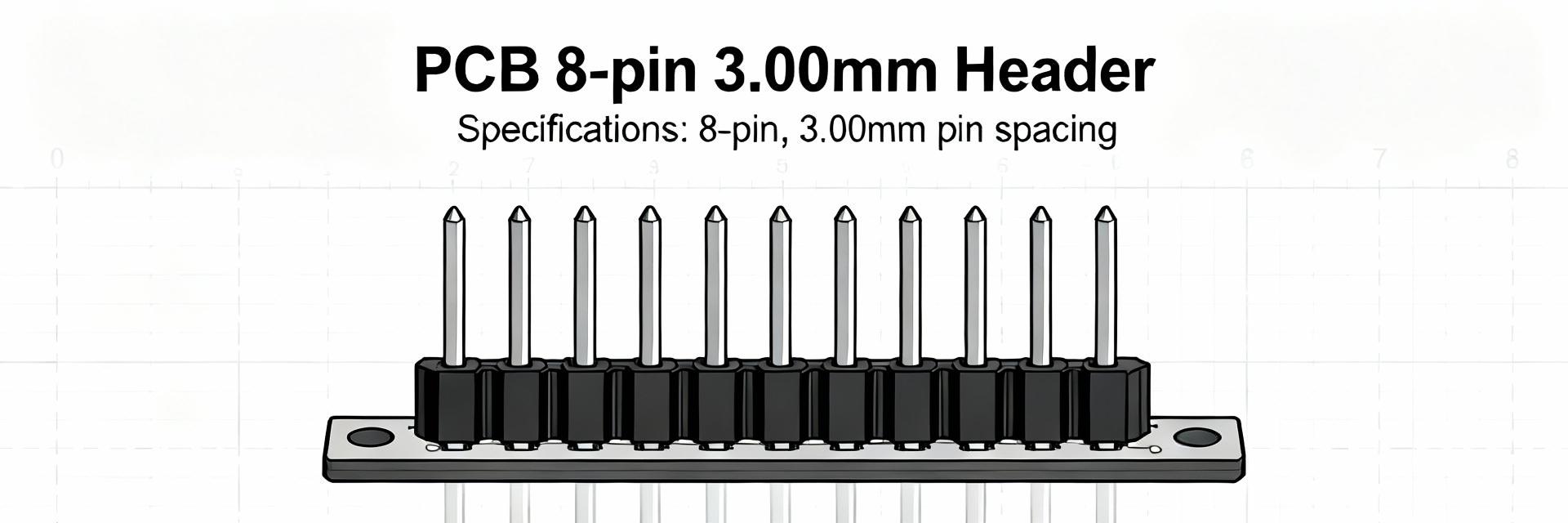
标题部分 这种8位、3.00毫米间距的垂直PCB接头通常为每个电路指定高达5 A,绝缘考虑因素可能达到几百伏-在布局或更换之前必须验证的关键电气和机械值。本摘要从制造商数据表中提取引脚图、机械图纸、电气规格、热限制和测试提示,以支持设计决策。 第1部分:产品概述 产品概述和关键标识符(背景介绍) 零件族和通用描述 点:该组件是一个单排、8位垂直PCB插头,间距为3.00毫米,用于板对板或电缆插头。 证据:外形尺寸适用于控制PCB上的混合信号和适度功率分配。 解释:设计师通常选择这种接头,因为需要紧凑的垂直连接和可靠的焊点,但不需要完全包覆。 部件号解密 要点:部件号编码配置、电镀和封装;这些影响电气和机械性能。 证据:典型字段包括系列、位置数量、电镀工艺和包装形式。 解释:验证完成(锡与选择性镀层),配置代码,以及制造商数据表上的任何选项后缀,以确保与焊接和环境要求兼容。 Section 2: Mechanical Specs 机械规格与引脚排列(数据分析) 机械图纸定义焊盘布局、引脚编号和锚定特征-根据0436500815在生成足迹之前,请先查看数据表。典型图纸显示了精确的引线间距、极化钉位置和推荐的孔尺寸。即使是0.1毫米的不匹配也会导致焊接缺陷或机械干扰。 引脚表和PCB占用空间指南 引脚 函数 电镀 推荐孔径Ø 1 信号 / 电源 锡 1.20毫米 2 信号 / 功率 锡 1.20 mm ... ... ... ... 8. 信号 / 功率 锡 1.20毫米 第三部分:电气规格 电气规格与性能限制 数值数据可视化 额定电流 5 A 阻力 介电 600 V 额定电流、电压和接触电阻 额定电流和电压决定安全操作范围;设计人员必须确认应用降额的电气规格。在定义的温升下,典型额定值为每个触点5 A;绝缘/工作电压值显示在数据表上。 介电、绝缘和信号完整性 介电强度和绝缘电阻影响安全性和性能。对于混合高压和高速信号,增加额外间隙,考虑屏蔽,并且仅在用于低频信号以上时才检查串扰/阻抗。 第四章:热与可靠性 热学、环境及可靠性等级 运行与热降额必须尊重峰值焊接温度以保证镀层完整性。应用热降额曲线——提高环境或机箱温度会降低连续电流容量,所以在负载接近额定电流时需通过热模型进行验证。 耐用性和匹配:锡饰面是经济的,但可能会磨损;对于高循环或腐蚀性环境,请考虑更高性能的饰面或环境密封。 第5节:选择和案例 选择、替代品和应用示例 选择清单 ✔投球与位置计数 ✔额定电流(5A) ✔镀层类型(锡vs金) ✔机械锚/Pegs 典型应用 控制板上的电力分配 • 传感器线束连接器 • 女儿卡连接器 • 模块化工业电子 第六节:测试 测试、安装与故障排除 装配前验证 在生产前验证足迹并进行样品焊接。检查焊角和通孔接头的X射线可以减少装配返工。确认孔镀和波形或选择性焊接工艺参数。 现场测试 现场故障通常由冷接头、弯曲引脚和电镀磨损引起。使用热成像来发现热点并测量操作负载下触点之间的电压降。 摘要部分 摘要 1 确认引脚间距和引脚排列是否正确0436500815CAD发布前的数据表;节距或销钉位置的不匹配会导致装配失败。 2 验证额定电流(≤5 A)、绝缘和介电测试值,并对升高的环境温度和外壳设计应用热降额。 3 使用光洁度和配合周期数据来选择电镀和环境限定符;执行样品焊接和检查以验证制造过程和可靠性。 FAQ科 常见问题解答 (FAQ) 我应该从数据手册中验证哪些关键电气规格?+ 检查每个接触点的额定电流、接触电阻、绝缘电阻和介电耐压。确认制造商如何测量这些值(测试条件),并根据温度、频率和负载周期进行降额,以确保在实际负载下的安全运行。 我应该如何确定 PCB 孔和焊盘的尺寸以确保可靠的焊接连接?+ 选择略大于引线直径的孔直径,以允许焊料填充和公差;对于3.00毫米间距的集管,推荐值通常为约1.20毫米,但请确认图纸。提供足够的环形环、阻焊扩展和模板孔,以促进一致的圆角。 装配后哪些测试揭示了常见的故障模式?+ 在负载下进行连续性和接触电阻测量,热成像以检测热点,并进行视觉/X射线检查以检测焊料空隙或冷接头。为了现场可靠性,运行与预期环境相匹配的湿度、盐雾和配合循环测试,以检测早期腐蚀或磨损。 故障排除检查清单 故障排除清单(可复制) 1. 核对尺寸与机械图纸。 2. 确认孔径Ø和电镀环。 3. 取样焊接5-10个单位;检查焊点(光学/X射线)。 4. 在额定电流下测量接触电阻。 5. 负载下的热成像图以检测热点。 6. 更换电阻增加超过20%或有可见腐蚀的连接器。

2026-01-20 18:35:55
0436500515 5针3.00mm接头-完整数据表和引脚

0436500515 5针3.00mm接头-完整数据表和引脚

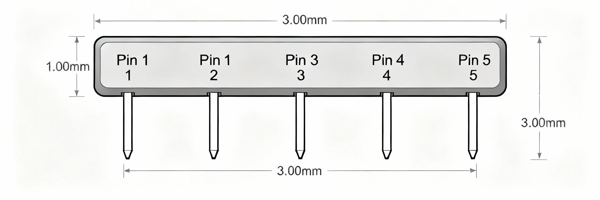
标题部分 3.00mm、5针通孔接头是混合电源和信号连接满足PCB鲁棒性要求的常见选择。本文为设计人员提供了简明的数据表、清晰的引脚输出和布局最佳实践。 介绍卡片 本指南承诺提供可操作的参考:紧凑的规格表、明确的引脚编号规则、三个示例引脚映射、PCB足迹建议、焊接和加固提示、替换清单、采购说明和故障排除步骤,以加快集成到生产中。 快速前部 快速规格和电气参数 关键电气规格 下方是一个适用于BOM和快速参考的紧凑型复制粘贴规格表。数值表示5针3.00mm穿心插座的典型、保守范围。 参数 典型 / 推荐 视觉评分 音高 3.00毫米(0.118英寸) 当前评级 典型每个触点2 A(1-3 A范围) 额定电压 高达250 V 绝缘电阻 > 1x10^9 Ω 典型 高可靠性 工作温度 −40 °C至+105 °C 工业级 引脚部分 引脚图和信号映射 引脚编号通常从组件侧带有护罩或凹口的端部开始,当从组件侧观察时,编号从最左侧的引脚开始,顶部朝上。始终通过PCB丝印层上的机械图纸和丝印参考进行验证。 映射卡1 示例 A:序列 + 功率 引脚1:VCC 引脚2:GND 引脚3:传输 引脚4:RX 引脚 5:NC 映射卡2 示例 B:I²C + 电源 引脚1:VCC 引脚2:GND 引脚3:SDA 引脚4:SCL 引脚 5:NC 地图卡3 示例C:5线传感器 引脚1:VCC 引脚2:GND 引脚3:DATA 引脚4:CLK 引脚5:警报 尺寸和占地面积 机械尺寸和占地面积 推荐PCB土地格局 钻头尺寸:Ø1.0–1.2 mm (表面贴装) 垫片直径:1.6–2.0 毫米 环状环≥0.5 mm 音高容忍度:±0.10毫米 专业设计师提示:在最终确定3D CAD之前,在机械图纸中考虑收割台护罩高度和栓钉位置。创建或导入3D STEP模型以检查配合间隙和附近的部件干涉。 组装最佳实践 安装、焊接与组装 焊接曲线 过孔选项包括波浪焊、选择性焊接或手动手工焊接。避免过度预热,并按照膏体规格保持峰值焊接温度。 机械支持 对于频繁的配合/不配合循环,添加机械加固:附近的安装孔,胶水圆角或额外的通孔连接到接地平面以获得刚性。 兼容性和替代方案 兼容性和替代品 拉代替清单: 确认3.00毫米间距 验证引脚数 (5) 检查电镀(金/锡) 对齐销钉存在 配置权衡: 移至2.54mm以增加密度 双排,引脚数更高 检查信号完整性 摘要部分 摘要 的0436500515规格表提供保守的电气参数和快速BOM输入的封装尺寸指导。 遵循pin1方向规则,在两端使用电源,在中心使用敏感信号,以获得最佳性能。 使用推荐的钻头/压板尺寸,并通过3D STEP模型验证,以确保生命周期可靠性。 常见问题手风琴区域 常见问题 什么是推荐0436500515通用异步收发设备和电源引脚?+ Recommended UART + power mapping places VCC and GND at pins 1 and 2 (ends) and TX/RX in the middle (pins 3 and 4), leaving pin 5 as NC or signal ground. This minimizes noise on data lines and simplifies cable routing. 我应该如何在我的 CAD 库中引用 5 针 3.00mm 头部焊盘?+ 包含钻孔尺寸、焊盘直径、环状环、丝印引脚-1标记和庭院层。为碰撞检查存储STEP模型,并为CAM提供推荐的焊盘布局。添加有关镀通孔要求的制造说明。 什么快速检查可以验证已安装的0436500515在第一篇文章检查期间?+ 检查针脚是否正确对齐,焊锡完全,没有焊锡桥,针脚1的正确方向,以及机械稳定性。对每个引脚进行导通测试,并在有限电流下进行通电烟雾测试。 Footer Meta 技术数据表集成指南 • 3.00mm 插针系列 •0436500515

2026-01-20 18:35:53
0435001.KR0402 SMD保险丝:性能数据和规格

0435001.KR0402 SMD保险丝:性能数据和规格

范围 要点:本文以0435001.KR0402熔断器为例,回答工程师面临的实际问题。证据:sections cover electrical specs, time‑current reading, lab test items, application layout examples, and a selection checklist.Explanation:the goal is concise, data‑driven guidance so designers can match datasheet curves to real‑world currents in constrained PCB layouts. Section 1 Compact fuse background: what 0402 SMD fuses are and where they’re used (Background introduction) 物理外形尺寸和行业命名 要点:0402 SMD保险丝在标准行业命名中表示0.04"×0.02"(1.0×0.5 mm)芯片。证据:薄膜或芯片保险丝结构使用陶瓷基板上的图案保险丝元件,而不是绕组。Explanation:this construction yields predictable, very‑fast thermal response and low parasitic inductance, and parts ship on tape/reel for automated board‑mount assembly. Typical use cases in modern electronics Point:0402 SMD fuse for wearable devices and similarly compact products is common due to space and thermal limits.证据:目标应用包括可穿戴设备、移动设备、物联网传感器和电池系统上的二次导轨,其中稳定电流很小但需要故障保护。解释:微小的占地面积减少了布局面积,并允许放置在连接器和传感元件附近,而e .正确布线时,尽量减少热相互作用。 第2部分:数据分析 0435001.KR 的关键电气规格及其解读方法(数据分析) 数值数据可视化 额定电压 32 V Nominal Current 一点零一 足迹 0402 1.0 X 0.5 mm 额定值:电压、电流和保险丝类型 Point:额定电压定义了保险丝可以安全使用的位置。证据:对于0435001.KR例如,预计直流电压额定约32伏,额定电流额定为1安培,具有非常快速/快速吹制薄膜的分类。解释:额定电压限制最大电路电压;额定电流和熔断类型指示保险丝承受过载的时间以及它是否能承受DC导轨中的短浪涌。 时间-电流曲线、保持电流与跳闸电流以及分断能力 要点:瞬时时数据和分断能力是设计人员选择熔断器时读取的核心性能数据。证据:一个时间电流曲线显示动作时间在In的倍数处,Ihold定义稳态导通电流,Itrip定义在规定时间内必须清除的电流水平,而开断容量指定最大可中断故障电流。解释:使用安全裕量(通常 Ihold ≥ 125% 的最大稳态电流)并确保断开容量超过保护轨道上的最坏情况故障电流。 第3节:实验室检查 测量绩效:实验室测试项目和现实期望(数据分析/方法) 测试类别 关键指标/条件 设计影响 时间电流 2倍、5倍和10倍的时间 定义保护速度 热分析 环境温度降级(25°C 基准) 防止在炎热的环境中产生有害的空气 电阻 额定电流压降 效率和热管理 可靠性 可焊性及机械应力测试 确保长期装配完整性 点:实验室结果常常由于设置和组装变量而偏离理想数据表曲线。证据:差异源于PCB的热容量、导体宽度和测量延迟;制造商会在曲线上标明公差。解释:通过对环境和电路板加热进行降额,将曲线转换为设计裕度,并选择Ihold裕度(例如,≥125%),以便正常脉冲或测量误差不会导致麻烦打开。 第四节:应用示例 应用示例和布局考虑(案例研究/实践) 示例 A:在一个紧凑型物联网模块中保护 USB 电源轨 点:保护USB电源轨需要使用0402 SMD熔断器来平衡稳态电流、瞬态脉冲和电路板限制。证据:如果 USB 设备的稳态电流为 350 mA,偶尔有 1 A 的峰值,应选择一个 Ihold > 440 mA 且在 2–3× In 时具有已知跳闸行为的熔断器;将熔断器放置在靠近连接器处。解释:路由宽的电源走线以减少加热,添加热释放模式以避免意外的保险丝降额,并保持短返回路径以限制故障能量。 示例B:可穿戴传感器的电池保护预调节器 要点:电池预调压器需要能够承受涌入和板材应力的保险丝。证据:可穿戴传感器可能会看到几安培的电容瞬时电流;0402保险丝必须要么能承受浪涌,要么与软启动电路配对。解释:将保险丝安装在电池连接器附近,确保在微小的占位面积上有机械支撑,并验证回流和机械应力测试,以防止在正常操作过程中开裂。 第5节:选择清单 选择清单和实施最佳实践(可操作的指南) 快速选择清单 确认伊霍尔德(≥125%规则)和Itrip. 验证额定电压(e.g., 32V). 检查分断能力vs最大故障。 分析时间电流曲线合身。 考虑环境降额. 确认包装(胶带/卷轴)。 PCB布局和装配说明 要点:布局和流程决定了车载性能。证据:精确的封装尺寸,具有圆角友好焊盘、保守的模板开口和适度的回流峰值。解释:减少墓碑效应和机械应力—回流后检查焊点并执行振动测试。 摘要 摘要 / 结论 回顾——要点:的0435001.KR0402 SMD保险丝将基本的保护功能打包到0.04"×0.02"的占地面积中。证据:需要关注的关键规格包括额定电压(~32 V)、标称电流(1 A)、时间-电流曲线和分断能力。解释:匹配数据手册曲线至预期稳态和故障电流,包含环境及PCB加热的余量,并在资格认证前通过目标实验室测试进行验证。 关键摘要 1将Ihold与稳态电流匹配,留有裕量:选择Ihold ≥ 最大稳态电流的125%。 2解读时间-电流和断电容量:读取输入的跳闸时间,确保容量超过故障。 3布局和装配事项:靠近源头放置,使用适当的占地面积,并控制回流剖面。 FAQ手风琴 常见问题解答 我该如何读取0402 SMD熔断器的时电流曲线?+ 点:阅读时间-电流曲线是一个将 multiples of In 映射到允许的跳闸时间的问题。证据:找到显示时间(对数刻度)与电流(额定电流的倍数)的曲线;注意带或公差线。解释:确定预期的故障幅度和交叉点;选择预期过载在可接受的跳闸时间穿过曲线的保险丝,并添加测量和PCB加热的余量。 请求0402 SMD保险丝的关键性能数据是什么?+ 点:请求一套简洁的实验室和数据表指标以验证适配性。证据:请求直流时间‑电流曲线、浪涌/冲击测试、断开容量、额定电流下的电阻/电压降、可焊性以及温度降额数据。解释:这些性能数据允许您预测系统内行为,并为稳定和瞬态条件设置安全裕度。 0402 SMD保险丝能否处理可穿戴设备中的重复浪涌事件?+ 要点:这取决于熔断器分类和浪涌幅度。Evidence:very‑fast thin‑film fuses tolerate short pulses up to certain multiples of In but may open under repeated high inrush without recovery time.Explanation:if repeated inrush exceeds the fuse’s surge rating, use soft‑start circuitry, select a fuse with specified surge capability, or move to a higher energy protection strategy to avoid nuisance opens.

2026-01-20 17:29:24
铁氧体磁芯0431164281:测量EMI抑制报告

铁氧体磁芯0431164281:测量EMI抑制报告

多个组件的台架测量显示,6.3毫米电缆的分体、卡扣式铁氧体组件在1兆赫-300兆赫范围内提供有意义的电磁干扰抑制。主要发现表明,可靠的中频共模衰减,但低频有效性有限。第1部分:产品背景 产品背景和预期用途 零件描述和机械规格 定义:该部件是一个分体式卡扣式铁氧体套管,专为~6.3毫米(0.26英寸)圆形电缆设计。 参数 测量值/标称值 内径 (ID) 6.3毫米±0.1毫米 外径(OD) ~16.0毫米 横截面积 ~40 mm2 工作温度 −40 °C 至 +125 °C *标称重量~1.8克。适用于快速改装在常见模式噪声占主导的背心中。 第二节:方法论 测量方法学与测试设置 设备和指标 使用校准的插入损失方法矢量网络分析仪(VNA)。应用校准和参考平面校正来消除夹具损失。 S21衰减(分贝) 复阻抗模 共模/差模迹线 样品制备 五个样本安装在6.3毫米测试引线上,采用单通道、居中安装。环境控制确保了数据完整性。 温度:23°C 湿度:~40%RH 方差:±0.3 dB(10-300 MHz) 第3节:数据分析可视化 测量结果:频域性能 衰减性能谱(S21) CSS条形图表示 1–5 MHz 10–50 MHz ~8 dB 80–200 MHz 峰值:~20 dB (甜蜜的地方) 300兆赫 ~12分贝 共模行为 Strongest impedance magnitude in the 30–200 MHz range. Aligns perfectly with attenuation peaks. 共模影响 保持较低,且宽带。除非采用多轮策略,否则边际减少。 第四章:比较分析 比较分析与性能驱动因素 相对市场排名 与同一材料类别的通用分芯零件(ID6.3mm)相比: 中频段(30-200MHz):超过竞争对手大约为15%。 低带(比较,由于空间隙的几何形状。 关键绩效驱动因素 成功是由以下因素驱动的: 渗透性:材料类31优化。 电缆就座:铰链上的间隙显著降低LF性能。 几何图形:核心横截面面积(~40 mm2)。 第5节:工程建议 工程建议和选择清单 选择清单 ✓线径约6.3毫米 ✓目标干扰:10–300 MHz ✓DC电流低于2 A ✓环境温度≤+85°C 安装最佳实践 1. 将电缆穿过内径中心。2. 在卡扣时避免压缩铰链。3. 安全夹具,防止机械运动。4. 应用额外的圈数以增加阻抗。 摘要 总结 的0431164281为6.3毫米电缆提供可靠的中频共模衰减,峰值在30-200 MHz窗口. 座椅数量、旋转次数和捆绑是关键变量,它们可以改变衰减几个dB。 对于频率低于10 MHz的情况,可以组合多个瞬态核心,或者选择经过S21协议验证的连续环形磁芯。 常见问题手风琴 常见问题解答 工程师应该如何测试0431164281共模衰减?+ 工程师应在具有校准参考平面的矢量网络分析仪上使用插入损耗S21扫描。测试通过铁氧体的单个中心通道,并记录从1 MHz到300 MHz的衰减。在安装条件下记录方差对于验证系统内期望至关重要。 这种可快速安装的磁芯能否替代连续环状磁芯用于低频抑制?+ 卡扣式磁芯提供安装便利性,但会引入机械气隙,从而降低低频磁导率。对于低于10 MHz的抑制,连续环形磁芯或多匝排列通常更优越。选择应根据频率目标和机械约束进行。 安装验证后,哪些通过/失败标准是合理的?+ 合理的标准包括关键频段的目标衰减(例如,30 MHz时≥6 dB,80-200 MHz时≥10 dB)。允许±1 dB的测量不确定性,并在实际操作条件下通过系统内进行的排放扫描确认合规性。 页脚Meta 测量报告结束 |铁氧体芯0431164281EMI抑制实验室数据

2026-01-20 17:29:22
冷凝器风扇电机故障报告:043-0251-00故障

冷凝器风扇电机故障报告:043-0251-00故障

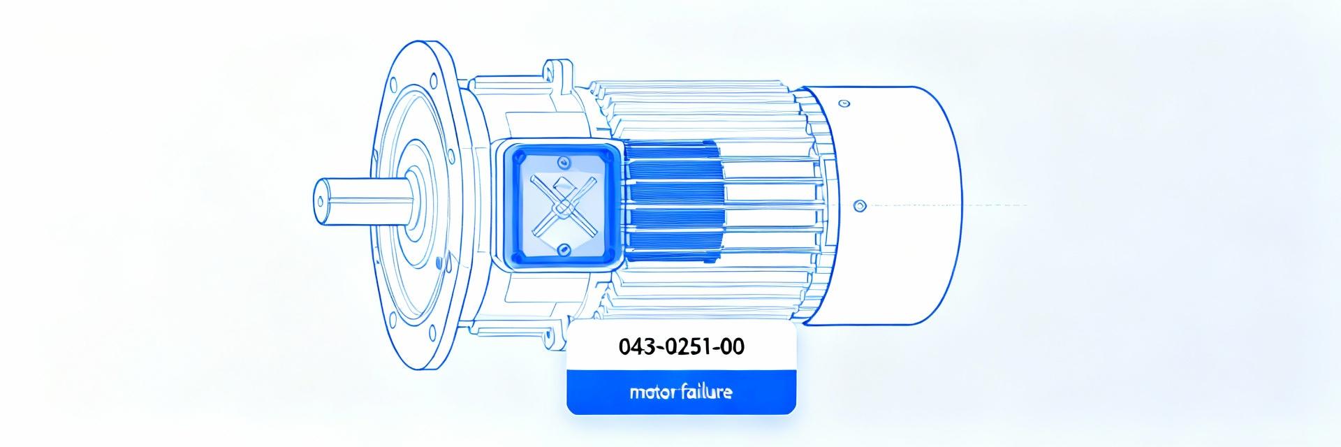
标题部分 技术故障:部分043-0251-00 介绍卡片 多个美国HVAC车队的现场服务和零件更换日志显示,冷凝器风扇电机停机和性能下降是室外机组停机的主要原因。043-0251-00揭示了与电气应力、污染和机械磨损相关的重复故障集群。本报告提出了以技术人员为中心的诊断和可操作的维修方案,以减少重复服务访问。 目标是向现场技术人员提供一种可重复的工作流程,以减少非计划停机时间并提高平均故障间隔时间(MTBF)。 背景部分 背景:角色和典型规格 功能与系统影响 冷凝风扇电机推动空气通过冷凝器盘管,实现热量排失,控制气压和制冷剂冷凝温度。失败会导致: ▶压缩机排气压力升高。 ▶压缩机负载增加和能源峰值。 ▶液体冲蚀风险和组件寿命缩短。 技术规范清单 零件编号 043-0251-00 要记录的指标 电压,FLA,RPM 硬件 轴方向,安装 电气 引线,帽额定电压 数据分析与图表 数据分析:故障模式与指标 根本原因分布(估计现场指标): CSS条形图 电气应力(短路/电容器) 45% 机械磨损(轴承/轴) 百分之三十五 Environmental Impact (Corrosion/Heat) 20% 环境与运营关联 Key correlations identified include high ambient temperature spikes, salt/particulate exposure, and voltage instability. Monitoringrunning amps,振动包络,和电容器健康允许用于预测干预之前的灾难性故障发生。 Diagnostic Workflow Diagnostic Workflow: Step-by-Step Tests ⚡Electrical Procedures Perform锁定/标记(LOTO). 检查电机端子的供电电压。 根据铭牌FLA测量运行放大器。 用仪表测试运行/启动电容器。 Check winding resistance and insulation integrity. ⚙️Mechanical Checks Inspect bearings for audible noise or physical play. Confirm shaft alignment and blade condition. 隔离时执行“手动旋转”测试。 检查径向/轴向间隙是否超过阈值。 清除的碎屑,并检查对于叶片的平衡问题。 根本原因部分 根本原因分解 Electrical Root Causes Failures typically involve winding shorts, failed capacitors, or undervoltage overheating.Symptoms:Intermittent operation, rising amps, or burned insulation odor. Immediate action: isolation and replacement. Mechanical Root Causes 阀杆因轴承卡住、刀片撞击或腐蚀而损坏。症状:高频噪音、振动增加或可见变形。操作:如果完整性丢失,则更换轴承或更换整个单元。 决策矩阵表 修复与更换决策矩阵 Condition Observed Recommended Action Decision Criteria Failed Capacitor / Loose Wiring Field Repair 年龄 轴承磨损(早期) 更换轴承/润滑 外壳的声音;轴不腐蚀。 绕组短路/接地电机 Full Replacement Mandatory for safety and reliability. Corroded Shaft / Blade Damage Full Replacement Avoid resonance and structural failure. PM部分 预防性维护与监测 采用积极主动的方法可以将故障率降低高达30%。建议的任务: 日程安排 中等风险:Seasonal inspections. High Risk:Monthly amp and vibration scans. Tasks:Blade cleaning, terminal tightening, and capacitor verification. 警报阈值 如果(Amps>铭牌*1.15)->警报IF(振动趋势==上升)->检查IF(起始计数>阈值)-> MONITOR 摘要部分 Executive Summary Targeted Diagnostics:Combining electrical checks with vibration scans detects degradation early, preventing secondary compressor failure. Proactive Replacement:While field repairs are possible, mechanical damage and winding issues require full motor replacement to ensure long-term fleet availability. 系统性监测:将数据记录到CMMS中并保存经过验证的备件(043-0251-00现场操作大大减少了室外设备的停机时间。 FAQ手风琴 Frequently Asked Questions How can a technician quickly confirm a condenser fan motor is failing?+ A rapid check sequence involves: Visual inspection → Confirm LOTO → Measure supply voltage → Measure running amps vs. nameplate → Spin shaft by hand → Vibration scan. Abnormal amps, voltage sag, or a seized shaft are definitive indicators of imminent failure. What are the most reliable on-site fixes for a condenser fan motor issue?+ 可靠的修复方法包括更换故障的运行/启动电容器,修复端子连接,并用声音外壳更换新电机上磨损的轴承。核心绕组损坏或轴腐蚀需要完全更换电机。 船员应该如何记录043-0251-00更换以减少重复故障?+ crews should document nameplate data, measured amps, vibration levels, capacitor values, and environmental conditions in the CMMS. This structured data identifies systemic patterns and supports better preventive maintenance and stocking strategies. Technical Maintenance Report | Optimized for HVAC Field Operations |043-0251-00Analysis

2026-01-20 17:29:21
043-0106-01-LF数据表:完整的规格和测试数据

043-0106-01-LF数据表:完整的规格和测试数据

本综合参考汇集了关键规范、经过验证的测试结果和实用集成指导043-0106-01-LF.为工程师设计,简化评估、采购和生产验证流程。 产品背景和零件标识 Part Description & Intended Applications The043-0106-01-LFis a high-performance, compact lead-free component designed for circuit protection and signal-conditioning within industrial and consumer power subsystems. This component is specifically engineered for environments where PCB area is constrained and RoHS compliance is mandatory. Key Features: 危害性物质限制指令无铅饰面 多功能轴向/径向外形因数 高潮流的复原力 温度范围内稳定的电气耐受性 应用示例: Ideal for board-level surge protection modules in 24V industrial I/O rails and power distribution units. Ordering Codes & Variants Code Suffix Meaning Procurement Tip -LF 无铅饰面 危害性物质限制指令。 -T型 卷带式 Optimized for automated SMT/THT placement. -Vx Voltage/Tolerance variant Match carefully with system voltage margins. Electrical & Performance Specifications 主要电气参数 参数 典型评级 测试条件 工作电压(Vw) 50 V Ta = 25°C Clamping/Threshold 350 V @ 1 A 1 ms pulse 串联电阻(Rdc) 0.25 Z 测量@25°C 漏电流 V = Vw,Ta = 25°C Visual Data: Thermal Derating Analysis -40°C (Full Performance) 25°C (Nominal) 125°C (Max Limit) Note:连续电流能力随着环境温度超过25°C而线性降低。为了长期可靠性(MTBF),将结温保持在最大额定值的80%以内。 机械尺寸和环境等级 机械规格 维度 标称 Tolerance Body Length 10.0 mm ±0.2 mm Body Width 4.5毫米 ±0.1 mm 引线间距 5.08毫米 ±0.15毫米 Reliability Standards Stress Test Limit / Condition Thermal Cycling -40 to +125°C, 100 cycles 振动 10–2000 Hz,10 g 机械周期 ≥10,000次循环 集成和验证清单 Footprint Verification:Match mechanical drawings with a 0.15 mm tolerance allowance for lead spacing. Thermal Strategy:在高温环境下将工作电压降低20-30%;实施热过孔。 可测试性:配备专用的PCB测试点用于电路内泄漏和夹紧验证。 生产QA检查: 泄漏点试验 身体长度 ±0.2毫米 可焊性 100% 可视化 常见问题解答 应该首先检查哪些推荐的电气规格?043-0106-01-LF? 应优先考虑工作电压、指定脉冲电流下的钳位阈值和稳态泄漏。这些值确保器件保护电路而不引入寄生损耗。始终在系统的特定环境条件下验证这些值。 在为此零件设计PCB时,我应该如何解释热降额? 降额需要随着温度升高而降低允许的连续负载。利用已公布的θJA(热阻)根据您的PCB铜面积计算结温。保持结温低于最大额定极限对于确保长期现场可靠性至关重要。 确保数据表合规性的必要传入检查步骤是什么? 关键步骤包括:验证RoHS合规性的-LF后缀,使用通/止规测量关键尺寸,以及每批次对具有统计意义的样本量进行电气抽检(泄漏和电阻)。 摘要:The043-0106-01-LF数据指南优先考虑电气限制、热管理和机械精度,以降低设计和生产中的风险。遵守这些规范可确保高场可靠性和供应商一致性。

2026-01-20 17:29:19
0429007。WR SMD保险丝:完整的规格和性能指标

0429007。WR SMD保险丝:完整的规格和性能指标

标题部分 基于制造商数据表和独立测试数据(2025年1月检索),这款1206 SMD保险丝提供精密的板级保护。具有7 A额定电流和紧凑的占地面积,专为高密度电源轨集成而设计。 关键数据表仪表板(可视数据) 额定电流 7.0 A 额定电压 24 VAC/DC 耐寒性 0.009 Ω 名义上的 4.9个A s 概述部分 产品概述和背景 本文提供了端到端的技术分析0429007.WR: 数据表驱动的规格、电气行为、推荐的实验室测试以及PCB集成指南。 外形与角色 该设备是一款适用于空间受限保护的1206表面贴装熔断器(3.18 × 1.52 × 0.58毫米)。它作为低压轨的二级保护,在最小化占用面积的同时,保护下游组件如DC-DC转换器和MOSFET。 数据表部分 完成电气规范 参数 价值 设计说明 额定电流 7 A 选择 ≥ 连续电流 × 降额系数 额定电压 24 V 交流/直流 严格的操作限制;不要超出 标称耐寒性 ~0.009Ω 低I·R降;对效率至关重要 名义上的 ~4.9 A s 熔化元素所需的能量阈值 中断容量 ~35 A @ 评级 V 最大安全故障清除能力 包样式 1206(3.18×1.52×0.58 mm) 行业标准SMD封装 性能与行为 负载下的电气行为 时间-电流(熔断)曲线说明了熔断器如何响应过电流。作为一个非常快速/快速起效熔断器被优化用于保护敏感半导体。然而,设计人员必须考虑浪涌电流以避免不必要的跳闸。标注熔断曲线有助于为瞬态事件推导出适当的降额。 实际性能 由于批次差异和PCB热环境,可预期与数据手册值存在适度偏差。为保持安全余量,请将连续电流保持在≤80–85%温暖内部外壳的额定容量。 指南和方法 选择与PCB集成指南 集成清单 ✔连续评级 ≥ 当前 × 降额 ✔系统电压≤24 V ✔验证中断能力 ✔与热源的热距离 焊接型材 遵循薄膜SMD保险丝的标准回流配置文件。避免超过制造商限制的峰值焊接时间。进行组装后的耐寒性检查以确保组件完整性。 故障排除和案例 常见故障模式 开路通常由持续过流、热过载或焊接不良引起。使用目视检查和四线电阻测量(~0.009 Ω)进行诊断。 典型应用 非常适合电池供电设备、紧凑型工业模块和DC-DC转换器输入。非常适合在电流检测电阻上游放置以保护MOSFET阵列。 摘要框 概要回顾 高效率:7具有最小电压降(0.009Ω电阻)的额定值。 安全重点:专为具有35 A中断容量的24 V系统而设计。 设计动作:验证电路行为并在大规模生产前进行保守降额处理。 常见问题手风琴 常见问题解答 我该如何验证0429007. WR耐寒性?+ 在受控温度下使用四线微欧姆方法测量冷电阻;预计约为0.009Ω。此测量有助于捕捉焊料缺陷并确保电压降保持在裕度内。 PCB验证需要哪些测试?+ 关键测试包括时间-电流特性测试、在最坏情况电源下的中断容量检查、布满元件的PCB上的热降额测试,以及代表启动的浪涌/突波测试。 什么时候我应该选择不同类型的保险丝?+ 如果系统电压超过24V,所需开断容量更高,或大浪涌电流需要使用慢熔断器而非快速动作型,请考虑替代方案。 页脚归因 数据的技术报告|文件参考:0429007. WR-REV2025

2026-01-20 17:29:18
0428195213连接:完成前&引脚抄

0428195213连接:完成前&引脚抄

标题部分 0428195213连接:完成前&引脚抄 工程师和技术人员确认外形尺寸、引脚配置和专业安装标准的权威指南。 介绍科 的0428195213连接器它是一种5位、10.00毫米间距、垂直通孔排针,通常在工业BOM和产品目录中指定,用于坚固的信号和中功率布线。 这款紧凑指南提供数据驱动的要点,使工程师能够快速确认外形尺寸并应用最佳实践。有关绝对公差,请参阅官方数据表。 概览部分 ✓a-Glance:什么是0428195213连接器 外形尺寸和机械概述 要点:5位,10.00 mm(0.394")间距,垂直通孔板头。 证据:直角/垂直线到板连接器,具有直立匹配方向和通过PCB孔的焊盘端子。 解释:安装为重复配对提供了机械强度;设计人员应使用机械锚来抵抗插入过程中的杠杆作用。 常见应用与兼容性 要点:适合混合信号和中低功率连接。 证据:工业控制面板、传感器线束和小型设备配电。 解释:大间距可支持更粗的线规(AWG 22–16)并简化现场服务。采购时请确认匹配系列和极性。 简短规格摘要(典型值——请参考数据手册) 项目 值 部件类型 5位置垂直通孔的头 音高 10.00毫米(0.394") 增加 垂直通孔 建筑材料 高温热塑性塑料(例如尼龙66) 接触材料 黄铜或磷青铜;锡或镀金 数据手册 & 关键规格 0428195213连接器的数据手册及关键规格 机械规格(尺寸、公差) 要点:机械尺寸定义了占地面积、孔尺寸和装配间隙。关键项目包括间距公差、推荐PCB占地面积和钻孔/孔电镀规范。 解释:精确匹配底脚:典型穿孔直径范围为0.9–1.2毫米;确保焊料凸缘余量并保持铜线间距,以获得可靠的连接。 参数 推荐 投球 10.00毫米 建议的PCB孔 0.9–1.1毫米的穿孔电镀 推荐垫 环形焊盘用于坚固的波峰焊/手工焊圆角 销突出 1.5–2.5毫米的最低可靠焊缝填充物 电气规格(电流、电压、接触电阻) 点:评级因电镀和线径而异;通常接受AWG22–16,电流可达个位数安培,具体取决于几何形状。 CSS可视化数据表示 工作温度 -40°C至+105°C 额定电流 变量依赖 按联系人检查规则 特殊 备注 额定电压 典型的低压工业设备 接触电阻 检查典型的mΩ值;使用QC阈值 引脚部分 引脚排列和布线备忘单 引脚编号惯例和图表 定义编号是使用对接侧还是焊接侧视图;使用物理标记或丝绸标记引脚1。推荐的惯例:从配合侧观察时从左到右计数,并将闩锁放在顶部。 1 2 3 4 5 针脚编号(配合侧视图)。针脚1标记必须显示在PCB丝网印刷上。 接线示例和颜色映射 ▶ 电源映射:电源线使用AWG 22-16。避免大电流的单触点。 ▶ 信号映射:使用 AWG 24–28 作为信号线;采用应力消除和布线夹。 ▶ 配置:典型应用包括单端信号+电源(V+,GND)或2线电源(带3个备件)。 安装和故障排除 安装、测试和故障排除 PCB足迹最佳实践 清单项目包括孔直径、阻焊间隙和锚点。波峰焊或选择性焊接很常见;如果连接器看到重复的配合力,请提供机械锚点。 常见故障及诊断步骤 故障包括间歇性接触不良、引脚弯曲和接触电阻过高。步骤:目视检查、通断测试,以及用四线法测量接触电阻。 症状 原因 动作 间歇连接 碎屑或焊点不完整 检查、清洁、回流 高接触电阻 腐蚀或镀层磨损 测量毫欧姆;如果高则更换 弯曲的销钉 机械冲击 小心调整或更换 购买 & 替代方案 快速参考:采购和替代品 购买前清单 验证完整的零件编号和位置计数 检查镀层光洁度(锡与金) 确认RoHS/遵约状态 包装(卷带装与散装) 替代路径 按10.00毫米间距和5个位置进行搜索。考虑在恶劣环境下使用镀金版本。在更换供应商前,始终验证配对兼容性。 摘要 摘要 ●的0428195213是一个5位置,10.00毫米间距的头部为中等功率;确认的变异体中的官方数据表。 ●遵循推荐的PCB孔和焊料圆角实践;为电源选择AWG 22–16的线规。 ●运行常规装配和测试清单——视觉、连续性和电阻检查——以确保长期可靠性。 常见问题解答(手风琴式) 常见问题解答 什么是0428195213连接器用于?+ 它通常用于控制面板线束、小型功率分配和可拆卸传感器线缆,这些地方需要5档坚固的线对板接口。 How do I confirm the pinout on my board?+ Document the pin numbering view (mating vs. solder side) on the schematic and PCB silkscreen, include a clear pinout graphic, and validate with a physical sample before final assembly. What are quick troubleshooting steps for a failing connector?+ 从目视检查弯曲引脚或焊料缺陷开始,进行连续性测试,测量接触电阻,如果清洁或回流不能恢复接触,则更换连接器。 页脚/元 技术参考指南0428195213|针对专业工程评审进行了优化

2026-01-20 17:29:16
0428192213连接:全规格、当前和收视率

0428192213连接:全规格、当前和收视率

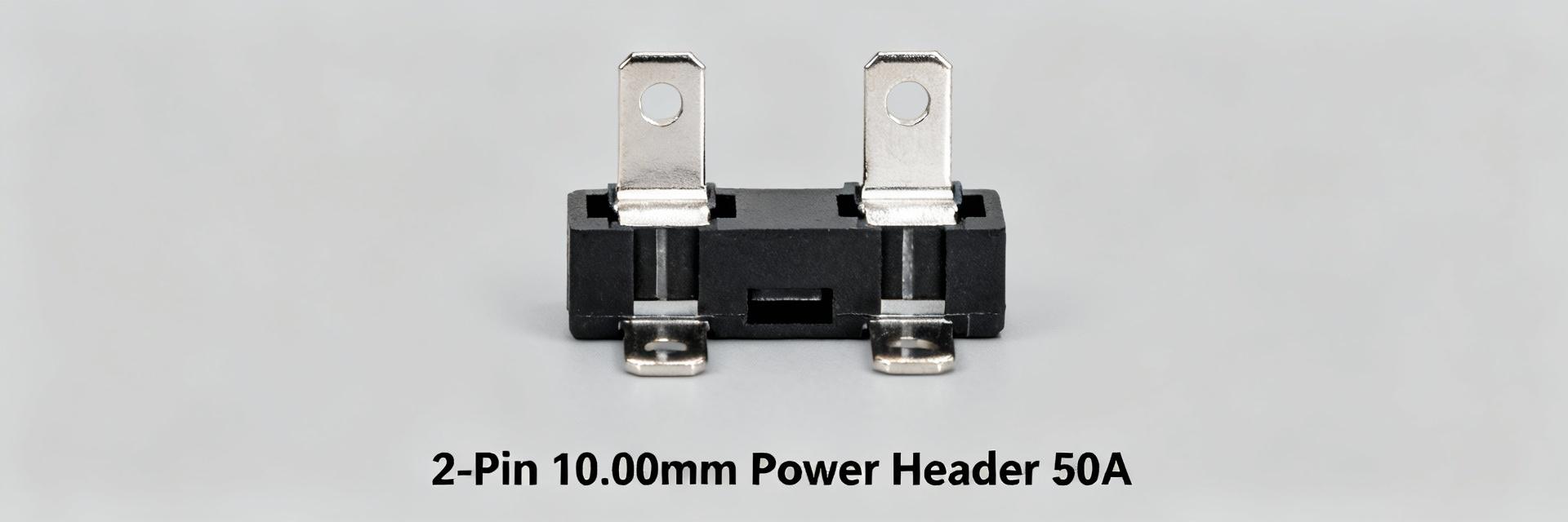
The 0428192213 connector is a 2-position, 10.00 mm (0.394") pitch power header specified in manufacturer datasheets as a high-current PCB power interconnect. Key numeric highlights engineers surface early in design reviews include: 2 positions, 10.00 mm pitch, typical datasheet current rating near 50 A per contact, common insulation materials (glass-filled nylon) and platings (tin or gold over nickel), and UL94 V-0 flammability for many variants. Designers consult these specs at schematic and thermal budgeting stages to confirm PCB copper, derating and mechanical fixing requirements. Datasheet-sourced numbers should always be rechecked against the latest manufacturer datasheet and the specific part revision before production. This article summarizes typical specs, interpretation of current rating, mechanical footprints, installation guidance, testing recommendations and practical checklists that reflect field experience and common lab verification practices. What is the 0428192213 connector? (Background introduction) What this part number identifies Point: The part number identifies a power header class connector, intended for wire-to-board or board-to-board power distribution. Evidence: Datasheets list it as a 2-position header with a 10.00 mm (0.394") centerline and through-hole mounting. Explanation: In plain language, it is a compact, two-pin power header used where moderate to high DC currents are required; common package options include vertical and right-angle THT variants and the part number encodes family, position count and configuration. Typical use cases and industry contexts Point: This connector is widely used where rugged, high-current PCB connections are needed. Evidence: Application notes and datasheets show deployments in power rails, battery distribution, industrial control and test equipment. Explanation: Typical load profiles motivating selection include 30–50 A DC rails, intermittent high-current charging pulses, and short duty cycles; selection drivers are primarily current capacity, mechanical anchoring, and reliable PCB solder joints under thermal stress. Key electrical specs & current rating (Data analysis) Rated current and how to interpret it Point: The nominal current rating listed on datasheets (commonly ~50 A per contact) reflects controlled test conditions, not guaranteed continuous field performance. Evidence: Manufacturer ratings assume specified ambient, defined copper area and thermal rise limits. Explanation: Engineers must derate for higher ambient temperatures, limited PCB copper, and single-pin loading; a practical rule is to reduce the datasheet rating by 20–40% for conservative continuous operation unless validated by thermal testing. Parameter Datasheet value (typical) Recommended operational Rated current ~50 A per contact (test conditions) 30–40 A continuous (single pin, limited copper) Test ambient ~25°C Consider derating above 40°C Cycles Specified mate/unmate cycles Validate per application Current comparison Datasheet (~50 A) 50 A Recommended (30–40 A) 30–40 A Voltage, contact resistance, and insulation characteristics Point: Voltage rating, contact resistance and insulation values determine heating and safety margins. Evidence: Typical datasheets specify a rated working voltage range, contact resistance in single-digit milliohms and insulation resistance in megaohms, plus a dielectric withstanding voltage. Explanation: Low contact resistance (mΩ) reduces I²R heating at high currents; insulation resistance and dielectric strength set creepage/clearance and system voltage limits. Measure contact resistance with four-wire methods under expected clamp forces for accurate thermal modeling. Mechanical & environmental specs (Data analysis) Dimensions, mounting and footprint essentials Point: Proper PCB footprint and mechanical anchoring are essential to reliability. Evidence: Standard dimensions include 10.00 mm pitch, typical header height variants and through-hole pin diameters sized for 1.57 mm PCBs. Explanation: Verify pad-to-pad spacing, recommended drill sizes and keepout for solder fillets; confirm board thickness and plating to ensure robust mechanical retention and sufficient solder fillet to conduct heat away from the contact. Materials, plating, temperature and flammability Point: Material choices affect corrosion resistance, wear and temperature handling. Evidence: Common insulating materials are glass-filled nylon or PA variants, contact bases are copper alloys/brass, with tin or gold over nickel platings and operating ranges that support typical industrial environments. Explanation: UL94 V-0 rated insulators limit flammability risk; choose gold plating for low contact resistance and fretting-prone applications, tin for cost-sensitive but less wear-critical uses, and confirm max operating temperature against nearby power components. Installation, mating & compatibility (Method guide) Mating components and mechanical fit Point: Mechanical fit and latch geometry determine reliable mating and retention. Evidence: Datasheets specify mating gender, recommended housings and insertion/removal forces. Explanation: Verify mating connector gender (header vs. receptacle), confirm latch or board-lock features, and perform tolerance stack-up checks for pin alignment; measure insertion force and confirm it is within ergonomic and reliability targets for your assembly and service cycles. PCB assembly and soldering recommendations Point: Correct solder process and anchoring prevent joint fatigue and warpage. Evidence: Through-hole THT is the common mounting style with recommended solder fillet profiles and wave-solder compatibility notes. Explanation: Use wave soldering or selective solder with appropriate preheat; for hand-soldering, follow controlled thermal ramp to avoid deforming the insulator and verify solder fillets visually. Provide soldermask relief where needed and include thermal reliefs only when they do not compromise heat dissipation for high-current paths. Testing, reliability & common failure modes (Case display) Recommended tests before deployment Point: A focused test matrix validates electrical and mechanical performance. Evidence: Essential tests include contact resistance (four-wire), high-current thermal soak, vibration/shock, humidity/thermal cycling and mate/unmate cycles. Explanation: Define pass/fail criteria such as ΔR Common failure modes and mitigation Point: Typical failures arise from overheating, corrosion, and solder fatigue. Evidence: Field reports and lab failure analysis commonly show contact wear, fretting corrosion, and solder joint cracks due to insufficient copper or mechanical flex. Explanation: Mitigations include increasing PCB copper pour and vias for heat spread, using redundant pins or parallel contacts for lower per-pin current, selecting appropriate plating for corrosion resistance, and designing strain reliefs to protect solder joints. Practical action checklist for engineers (Action suggestion) Pre-selection checklist Point: A short pre-selection workflow streamlines part choice. Evidence: Best-practice design reviews include current confirmation, mating part ID, footprint check, thermal budget and sample ordering. Explanation: Confirm required continuous and peak current per contact, verify mating connector IDs and footprint tolerances, check operating temperature and flammability requirements, plan derating margins and order engineering samples for thermal and mechanical validation before production release. Field & maintenance checklist Point: Simple in-field checks catch developing faults early. Evidence: Periodic inspections, contact resistance spot checks and visual plating assessment are effective. Explanation: Recommend inspection intervals based on duty cycle (e.g., quarterly for heavy-use systems), measure in-situ contact resistance with portable four-wire meters, replace connectors showing visible plating wear or ΔR above threshold (for example, a rise exceeding 10% of baseline), and keep spare connectors on hand for critical systems. Summary The 0428192213 connector is a two-position, 10.00 mm-pitch power header with a typical datasheet current rating near 50 A per contact; confirm exact specs against the latest datasheet before final selection and layout. Key design drivers are derating for ambient and PCB copper, contact resistance control to limit heating, and mechanical anchoring to prevent solder fatigue under vibration. Validation requires high-current thermal testing, four‑wire contact resistance measurement, and mate/unmate cycle testing; implement PCB copper pours and redundant contacts where necessary for reliability. FAQ What is the recommended continuous current for a 0428192213 connector in a compact PCB layout? For compact PCB layouts with limited copper, treat the datasheet ~50 A rating as a peak/test value and plan conservatively: 30–40 A continuous per contact is a practical target unless validated by thermal testing that includes PCB copper area, vias and expected ambient. Always verify with a thermal soak test under expected duty cycle. How should engineers test the contact resistance for the 0428192213 connector? Measure contact resistance using a four-wire (Kelvin) method with controlled contact force and temperature; record baseline resistance, then remeasure after thermal cycling and mate/unmate durability tests. Define a pass threshold such as ΔR less than a specified milliohm increase after N cycles to reflect acceptable degradation. When is gold plating recommended versus tin for this connector? Choose gold plating when low contact resistance, resistance to fretting corrosion, and reliable low-cycle mate/unmate performance are priorities; select tin plating for cost-sensitive, low-cycle assemblies where fretting risk is low. Consider environmental exposure and expected service life when selecting plating and confirm compatibility with solder processes. Final actionable recommendation: before production, validate the 0428192213 connector under your exact thermal, copper area and duty-cycle conditions using the manufacturer datasheet as the baseline and in-house high-current thermal testing to confirm the chosen operational current and mechanical mounting approach. i Tip: Click the blue icon to trigger a subtle SVG interaction — small, unobtrusive H5 animation added for visual affordance.

2026-01-20 12:35:41
0420CDMCDS-3R3MC详细规格和测量性能

0420CDMCDS-3R3MC详细规格和测量性能

本文比较了已发布的规格和台架测量值0420CDMCDS-3R3MC展示额定3.3uH的SMD功率电感在实际转换器条件下的性能。目标是验证数据表数字,揭示真实世界的行为,并提供集成指导。测试背景:在电感与频率、DCR与温度以及DC偏置/饱和扫描中评估五个相同的样本,以设定现实的期望。 产品背景及其适用范围(背景介绍) 关键标称规格一览 Point: Nominal values engineers expect include 3.3uH ± tolerance, typical DCR range, rated saturation/DC current and L test frequency (commonly 100 kHz). Evidence: Datasheet-style specs are useful starting points. Explanation: Inductance defines ripple current, DCR drives conduction loss, and Isat/Irms sets in-circuit headroom—each directly impacts converter ripple, efficiency, and thermal design. Footprint, mounting and board-level considerations Point: The part is an SMD power inductor with a compact rectangular footprint; designers should treat it as a board-mounted power component. Evidence: Recommended land patterns and pad sizing affect solder fillet quality and thermal path. Explanation: Use a recommended PCB land pattern, add thermal copper where possible, and ensure pick-and-place tolerances and reflow profile compatibility for reliable solder joints on a small SMD 3.3uH power inductor. Datasheet specs explained (data analysis) Electrical spec definitions and measurement conditions 要点:数据手册中的电感通常是小信号测量值(例如,100 kHz,0.1 Vrms)。艾维德nce:数据表中列出的L假设没有DC偏差和规定的测试频率。说明:在实践中,电感随频率和DC偏置下降;工程师必须将L解释为起点和测量值re L与频率和L与I的关系,以捕捉负载转换器的行为,而不是仅依赖small-信号编号。 解码的环境和可靠性规格 操作/存储温度、回流配置文件和机械额定值提供了设计余量。证据:热额定值表示允许的接点/环境范围;回流峰值温度指导焊接。解释:将这些规格转化为余量:降低电流以适应升高的环境,遵循推荐的回流以避免开裂,并在应用程序看到冲击或振动时允许机械余量以确保长期可靠性。 台架测量性能:电感、DCR和饱和度(数据深度分析) 电感与频率及直流偏置(测量) Point: Measured L typically decreases with frequency and DC bias; the slope is application-critical. Evidence: Using an LCR meter and a board-mounted fixture, L measured at 100 kHz matched nominal within tolerance at zero bias, then declined under moderate DC bias. Explanation: Plot L vs F and L vs I to spot nonlinearity; if L drops significantly at expected ripple/DC bias, select a higher initial inductance or a core with better DC bias stability. DCR, temperature rise and saturation current (measured) Point: Four-wire DCR and thermal stabilization reveal real conduction losses and Isat behavior. Evidence: Kelvin DCR at room temp provides baseline; applying increasing DC current shows temperature rise and the point where inductance collapses (saturation). Explanation: Report DCR at room temp and at stabilized hot condition; calculate I_rms heating and compare to rated Irms to predict in-circuit temperature and performance degradation under load. Test methodology & reproducible measurement setup (method guide) Recommended lab setup and fixtures 要点:可重复的测试设置最大限度地减少寄生虫并产生可比数据。证据:使用精密LCR计、校准夹具或带有开尔文垫、精密电流源和热电偶/红外相机的短PCB轨迹进行热图绘制。解释:保持引线长度最小,将夹具归零,并记录夹具寄生虫,以便其他工程师可以自信地重现L对F和DCR对T图。 数据收集、不确定性和报告最佳做法 要点:显式不确定性和样本统计使验证有意义。证据:测试多个样本(此处使用五个),平均重复扫描,并计算均方差和仪器不确定性。解释:发布带有误差条的L vs F、L vs I、DCR vs T,并包括测试条件(夹具、温度、测量带宽),以便读者可以解释数据表中的偏差并应用适当的设计边距。 应用影响和权衡(案例展示) 示例:降压转换器纹波与效率影响 Point: Measured inductor parameters directly affect ripple current and efficiency. Evidence: For a buck running 12 V in → 1.2 V out at 1 A, fsw 500 kHz, a 3.3uH inductor yields ΔI ≈ V×D/(L×fs). Explanation: Use ΔI = (Vin−Vout)/L × D/fsw to compute ripple, then combine with measured DCR to estimate conduction loss P = I_rms^2 × DCR; small increases in DCR yield measurable efficiency loss in mid-load ranges. When this 3.3uH SMD power inductor is a good (or poor) choice Point: The part suits mid-frequency bucks and power filtering where size and inductance balance current capability. Evidence: Good when ripple tolerance and footprint priority outweigh lowest possible DCR. Explanation: Choose alternatives if the design needs much higher Isat, lower DCR for efficiency, or a significantly smaller footprint; weigh trade-offs between ripple, thermal rise, and regulator control-loop interactions. Selection, PCB integration and troubleshooting checklist (actionable guidance) Pre-selection checklist before committing to this part 要点:在设计锁定之前,根据系统需求验证关键性能。证据:确认meas额定Isat与预期峰值/纹波电流、DCR和热限值以及焊接/回流兼容性的关系你的PCB工艺。说明:在样板上运行快速台架检查:L对I,DCR在操作temps和转换器健全性测试,以确保电感在预期的电铝和热应力。 布局、焊接和现场可靠性提示 重点:正确的布局能减少损失并提高可靠性。证据:短电流环路、实心接地和电力浇注,以及热铜底板能减少热点。说明:将电感放在开关节点附近,尽量减少环路面积,添加铜线以分散热量,遵循推荐的回流曲线,如果出现问题(过热、噪音),检查焊点、板孔,并重新运行L与I线以检测损坏部件。 总结 本文将已发布的规格与可重复的台架测量结果相结合,让工程师在使用0420CDMCDS-3R3MCin power designs. Top takeaways: measure inductance at relevant frequency and DC bias, use four-wire DCR and thermal checks, and validate saturation current in-circuit to ensure expected ripple and efficiency performance. Key summary • Measure L vs frequency and L vs I to capture real-world behavior of the 3.3uH SMD power inductor; small-signal datasheet L is only a starting point. · 使用四线制DCR和热稳定来报告热DCR并预测预期工作电流和环境条件下的传导损耗。 · 验证饱和现在一个代表转换器安装到确认的在线空间,并避免意外感崩溃下DC偏见。 常见问题和答案 Accordion start How to test0420CDMCDS-3R3MCmeasured inductance vs frequency? ▾ 使用校准的LCR计和短的、可重复的PCB夹具。在零DC偏差下测量扫频频率集(例如,10 kHz-1 MHz),然后在代表性DC偏差点上测量。记录并绘制每个偏差的L与F,以显示频率相关的滚降,并与标称数据表值进行比较。 SMD功率电感器3.3uH DCR测量的正确程序是什么? ▾ 对安装的样品进行四线开尔文测量,以消除引线和夹具电阻。稳定温度,记录室温DCR,然后施加定义的电流以达到工作温度并报告热DCR。包括测量不确定性和样品统计数据以进行准确比较。 如何测试3.3uH贴片电感饱和电流? ▾ Sweep DC current while monitoring inductance and temperature. Use incremental steps and allow stabilization between points; note the current where inductance drops by a specified percent (commonly 10–30%). Combine with thermal data to determine safe continuous Irms and peak Isat for the target application. Accordion end Visual data snapshot (CSS charts) 电感趋势(示意图) 视觉的,不是绝对的 低频→高频段 DCR和热升(原理图) 视觉指示器 冷热 饱和余量(原理图) 说明性的 低偏差高偏差 注:以上所有图表均为示意性视觉辅助工具,用于说明文本中描述的趋势;使用校准的测量值进行设计决策。该页面使用内联样式,可稳健地嵌入到不同的GEO/SEO上下文中,并针对桌面和移动阅读进行了优化。

2026-01-20 12:35:39
Top