이것은LPC802M001JDH20Jis a purpose-built, ultra-compact 32-bit Cortex-M0+ MCU family member optimized for low‑power embedded designs; it advertises a maximum CPU clock of around 15 MHz, an entry‑level flash footprint, multi‑channel ADC and common serial interfaces. This introduction frames what the part actually delivers for US product and prototype workflows and points engineers toward the official datasheet for final verification.
Practical use favors tiny battery‑powered nodes, low‑cost consumer controls and compact sensor endpoints where package size and power dominate decisions. Read the official datasheet revision and errata before design lock: focus first on electrical characteristics, memory map and pinout to verify the exact specs for your chosen variant.
Why the LPC802M001JDH20J matters (background)
Target applications and product fit
Point: The MCU is aimed at minimal‑function, cost‑sensitive embedded products. Evidence: Typical fits include simple sensors, basic control nodes and battery‑powered IoT endpoints where MCU functions are modest. Explanation: Designers trade off raw compute and feature set for low BOM cost, small PCB area and low quiescent current—making this part a sensible choice for multi‑year battery targets and compact consumer devices.
공식 데이터시트 및 수정 노트
요점: 항상 공식 데이터시트 PDF 및 현재 에라타를 참조하십시오. 증거: 데이터시트에는 보드 레벨 결정을 결정하는 전기 테이블, 메모리 맵 및 핀 설명이 포함되어 있습니다. 설명: 제조업체의 웹 사이트 또는 공인 문서 포털에서 데이터시트를 가져오고, 문서 수정 및 에라타 ID를 확인하고, 전기적 특성, 메모리 매핑 및 핀아웃 페이지를 먼저 읽습니다. PCB 레이아웃 전에 패키지 변형 및 절대 최대값을 잡으십시오.
LPC802M001JDH20J: 주요 전기 및 메모리 사양 (데이터 심층 분석)
Core, clock and voltage specs
Point: Cortex‑M0+ core with modest maximum clock and a single‑supply domain suits low‑power designs. Evidence: The part targets a maximum CPU clock around 15 MHz with standard internal oscillator options and a single‑supply operating window typical for low‑voltage MCUs. Explanation: Clock and supply choices directly affect performance and current draw—lower clock and reduced core voltage yield proportional savings in active current, so configure clocks only as high as needed for the workload to maximize battery life.
Memory and storage layout
Point: Memory is sized for compact applications. Evidence: This family is an entry‑level flash class (typical devices in this family sit in the ~16 KB flash region) with a small SRAM block sufficient for lightweight stacks and buffers; boot ROM features often provide a minimal bootloader. Explanation: Flash and RAM limits constrain large frameworks and over‑the‑air images; keep firmware lean, use link‑time garbage elimination, and verify the exact flash/RAM numbers in the datasheet before committing to production.
LPC802M001JDH20J peripherals & interfaces breakdown (data deep‑dive)
아날로그 주변 장치: ADC 및 비교기
포인트: On 칩 아날로그는 기본 감지를 지원합니다. 증거: 선택 가능한 참조 옵션과 온도, 조명 및 배터리 감지에 적합한 소수의 채널이 있는 10-12비트 클래스의 다중 채널 ADC를 기대합니다. 설명: ADC 샘플링 전략이 중요합니다. 펌웨어 복잡성이나 전력 사용을 팽창시키지 않고 측정 정확도를 충족하기 위해 평균화, 적절한 기준 선택 및 입력 컨디셔닝
디지털 인터페이스: I2C, SPI, USART, 타이머, GPIO
요점: MCU는 일반적인 임베디드 작업에 필수적인 직렬 및 타이머 주변 장치를 노출합니다. 증거: 일반적인 오퍼링에는 I2C, SPI 및 하나 이상의 USART, PWM 기능이 있는 기본 타이머 및 핀 mux 제약 조건이 있는 GPIO가 포함됩니다. DMA는 일반적으로 엔트리 클래스 장치에 없거나 제한됩니다. 설명: 멀티플렉싱 핀에는 계획이 필요합니다. 충돌을 피하기 위해 지도 센서와 디버그 핀이 필요하며, 높은 대역폭 스트이 아닌 단일
성능, 전력 소비량 및 열 한계(데이터 분석)
Power modes, current draw and battery planning
Point: Power profiles determine battery life more than peak CPU speed. Evidence: Typical devices show low‑microamp deep‑sleep and modest active currents at low MHz; a simple battery‑life calculation uses average current = duty%*active_current + (1-duty%)*sleep_current. Explanation: Example: with 1% active duty, 5 mA active peaks and 5 µA sleep, average current ≈55 µA; a 2,000 mAh cell yields ~36,000 hours (~4 years) of theoretical life—use datasheet figures for accurate planning and include radio or sensor currents if present.
Small visual bar chart (CSS via inline styles)5mA
0.005mA
0.055 mA
Thermal, package and operating conditions
Point: Small packages limit thermal dissipation and continuous high‑current operation. Evidence: The part is available in compact 20‑pin small‑outline packages with standard commercial temperature ranges; continuous high‑power draw forces derating. Explanation: For sustained loads, follow the datasheet thermal guidance, avoid heating from nearby regulators or radios, and design for the worst‑case ambient to keep junction temperature within limits for reliable lifetime.
Hardware integration & PCB guidelines (method guide)
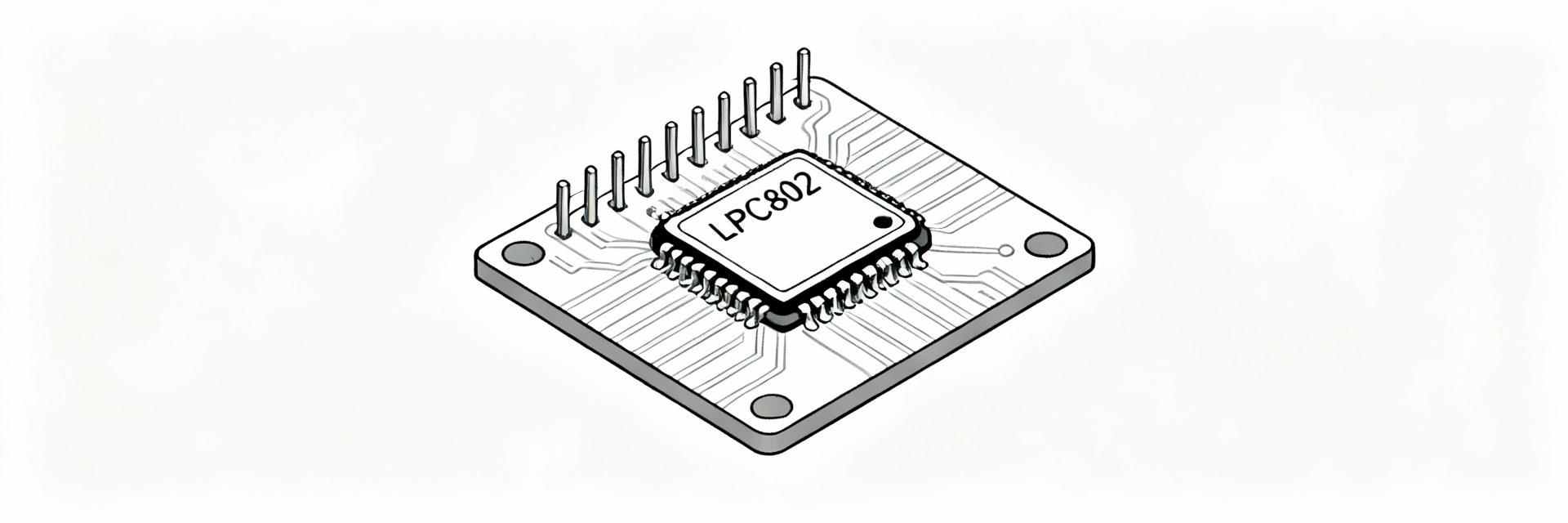
핀 아웃, 패키지 옵션 및 외곽설정 팁
포인트: 올바른 풋프린트 및 핀 할당은 재작업을 방지합니다. 증거: 중요 핀에는 20핀 핀아웃에 VDD, VSS, RESET 및 디버그 라인(SWDIO/SWCLK)이 포함됩니다. 작은 패키지는 라우팅 및 디커플링 배치를 제한합니다. 설명: VDD 핀 근처에 기본 0.1 F 디커플링 캐패시터를 놓고 RESET 및 디버그 트레이스를 짧게 유지하고 MCU 아래에 접지 주입을 예약하여 리턴 경로를 안정화하고 E
전원 공급 장치, 시계 및 재설정 회로 권장 사항
포인트: 간단한 전원 및 재설정 회로는 신뢰성을 향상시킵니다. 증거: 0.1 F 세라믹 디커플링과 VDD의 1 F 벌크 캡, RESET(10 k)의 풀업 및 Schmitt 트리거 입력을 사용하여 사용할 경우 외부 재설정을 수행합니다. 설명: 외부 오실레이터가 필요한 경우 크리스탈 또는 오실레이터 모듈에 대한 레이아웃 지침을 따르십시오. 그렇지 않으면 보정과 함께 내부 RC를 사용하여 구성 요소 수
펌웨어, 프로그래밍 및 개발 워크플로우(방법 가이드)
Bootloader, debug and programming interfaces
Point: Multiple programming paths simplify prototyping. Evidence: Devices typically provide a ROM boot path and SWD debug interface; flashing is possible with a standard SWD‑compatible tool using SWDIO/SWCLK plus VDD/GND and optional RESET. Explanation: During prototyping, keep SWD accessible and plan for a production debug header or programming pogo pad; verify minimal signals needed from the datasheet before wiring fixtures.
Minimal BSP & example start‑up sequence
Point: A compact startup saves flash and RAM. Evidence: Minimal init includes oscillator setup, GPIO defaults, ADC calibration and low‑power configuration. Explanation: Initialize clocks to the lowest frequency that meets timing, set unused pins to defined low‑power states, sample ADC only when needed, and use link‑time optimization and stripped C libraries to minimize footprint.
Application examples & design checklist (case + action suggestions)
3가지 간결한 예제 프로젝트
예 1: 배터리 환경 센서 - 주변 장치: ADC, I2C 온도/습도, 저전력 타이머, 예상 메모리: 소형 부트로더 + 소형 센서 스택(~8-16KB 플래시); 전원: 주기적 웨이크, 샘플, 전송, 딥 슬립 전략. 예 2: 간단한 모터/촉각 제어 - 주변 장치: PWM 타이머, GPIO, 소형 상태 기계; 메모리: 입력 디바운스 및 제어를 위한 적당한 펌웨어. 예 3: UART/I2C 브리지 - 주변 장치: USART 및 I2C, 최소 버퍼링, 낮은 처리량 브리
설계 및 구매 체크리스트
요점: 주문하기 전에 변형 세부 정보를 확인합니다. 증거: 첫 번째 체크리스트 항목: 공식 데이터시트를 입수하여 구매하려는 패키지 변형에 대한 정확한 부품 표시, 수정 및 세부 사양을 확인합니다. 설명: 또한 패키지 유형, 프로그래밍/디버그 어댑터 호환성을 확인하고 레이아웃 확인을 위한 샘플을 주문하고 생산 수량에 대한 공급 연속성을 보장합니다.
요약
-
TheLPC802M001JDH20Jis a compact, cost‑focused Cortex‑M0+ option for tiny, low‑power embedded designs; verify flash/RAM and electrical numbers in the official datasheet before committing.
-
Plan power early: use low duty cycles, minimal clocks, and accurate battery‑life calculations based on datasheet current figures.
-
Prototype with SWD debug access, correct decoupling and pin‑mux planning to catch layout issues before production.
