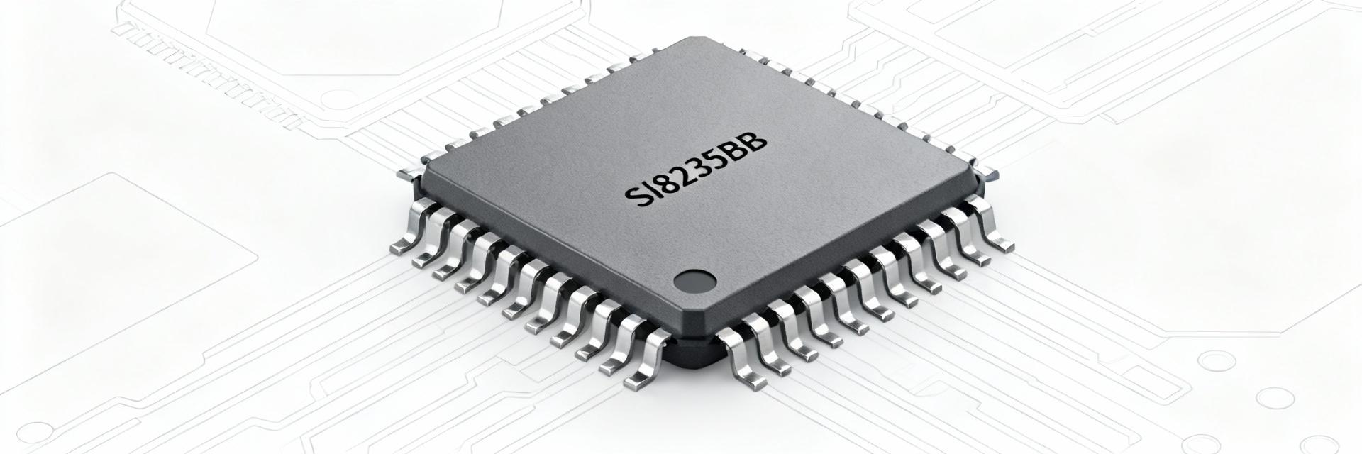
요점: SI8235BB은 약 4A 피크 드라이브와 ~2.5 kVrms 절연 성능을 갖춘 듀얼 채널 절연 게이트 드라이버로, 이는 중고전압 전력 단계에 적합함을 즉시 보여줍니다. 증거: 이 피크 전류와 절연 수치는 드라이버가 게이트 커패시턴스를 얼마나 빠르게 충전/방전할 수 있는지, 그리고 어떤 절연 엔실로프를 지원하는지를 결정합니다. 설명: 이 글에서는 해당 데이터시트 값을 측정 가능한 온보드 성능, 레이아웃 동작, 열 현실로 변환하여 설계자가 실제 컨버터와 모터 인버터의 동작을 예측할 수 있도록 합니다.
배경: 현대 전력 시스템에서 고립된 게이트 드라이버가 중요한 이유
격리, 안전 및 규제 상황
요점: 갈바닉 절연은 고전압 전력으로부터 저전압 제어를 보호하고 규제 크리프/간극 요건을 지원합니다. 증거: 2.5kVrms에 가까운 절연 등급은 강력한 유전 저항 능력을 나타내며 작동 전압 등급 및 PCB 크리프 간격을 설정하는 데 도움이 됩니다. 설명: 설계자는 목표 작동 전압 및 오염도 당 크리프/간극을 선택하고 배리어 트랙을 배치하고 적절한 슬롯을 배치하여 격리된 트 드라이버가 시스템 안전 및 서지 기대치를 충족하도록 격리 등급을
일반적인 토폴로지 및 기능적 역할
Point: Isolated gate drivers are used for half-bridges, full bridges and high-side gate drive where bootstrapping is inadequate or multi-level isolation is preferred. Evidence: dual-channel isolation consolidates two gate drives into one package, simplifying board routing and ensuring matched timing between channels. Explanation: In converters driving Si, SiC or GaN switches, a dual isolated driver reduces component count and eases layout in multiphase or bridged topologies while providing independent isolated supplies and balanced propagation behavior.
SI8235BB performance specifications overview
Key electrical specs to benchmark
Point: Engineers should benchmark peak output current (4 A peak), propagation delay, input-to-output isolation voltage, common-mode transient immunity (CMTI), UVLO thresholds, gate voltage swing and output fault behavior. Evidence: peak drive current governs how fast gate charge is delivered; propagation delay and skew determine timing margins; CMTI quantifies immunity to high dv/dt events. Explanation: Tracking these metrics during validation links switching losses, timing margins and transient immunity to observed device stress—enabling safe switching-environment specification and coordinated gate resistor selection.
Thermal, SOA and reliability considerations
포인트: 피크 전류 정격은 연속 능력과 같지 않습니다. 열 감쇠 및 패키지 열 저항은 안전한 연속 작동을 정의합니다. 증거: 반복 속도가 높은 드라이버 펄스는 PCB 구리, 바이아 및 대류를 통해 제거해야 하는 평균 전력을 생성합니다. 피크 사양이 강조되기 훨씬 전에 SOA 한계에 도달할 수 있습니다. . 설명: 스위칭 이벤트당 에너지, 주어진 스위칭 주파수 및 듀티 사이클의 평균 전력을 계산하여 피크 전류 기능을 실제 연속 구동으로 변환한 다음 PCB 열 경로 및 디레이팅을 사용합니다. 최대 지속 가능한 게이트 드라이브 활동을 설정하는 곡선.
비주얼 리포트/CSS 차트 표현빠른 시각적 표시기
Notes: bar widths are relative visual indicators for quick comparison; validate against full datasheet graphs for precise thermal/SOA limits.
SI8235BB 실험실 테스트 및 실제 성능
추천된 테스트 설정 및 측정 절차
요점: 정확한 측정에는 신중한 탐색, 제어된 디커플링 및 안전한 격리 관행이 필요합니다. 증거: 반환을 위해 짧은 접지 리드 또는 격리된 프로브를 사용하고, 고주파 디커플링 캐패시터를 공급 핀에서 밀리미터 이내에 배치하고, 적절한 고정 장치 간극으로 고전압 테스트 중에 격리를 유지합니다. 설명: 권장 절차: 대표적인 PCB에 DUT를 장착하고, 바이아로 접지를 꿰매고, 스코프 프로브 접지를 스프링으로 배치하거나 활성 프로브를 사용하고, 상승/하강 시간, 전파
결과 및 일반적인 고장 모드 해석
포인트: 데이터시트 값의 편차는 레이아웃 또는 공급 문제를 나타냅니다. 일반적인 고장에는 잘못된 전환, 열 폴드백 및 래치업이 포함됩니다. 증거: slower-than-expected 가장자리는 종종 과도한 루프 인덕턴스 또는 크기가 작은 디커플링에서 비롯됩니다. CMTI 고장은 큰 공통 모드 dv/dt 및 불충분한 차폐와 관련이 있습니다. 설명: 관측된 상승/하강 시간이 길면 트 루프 영역 및 디커플링을 검사하십시오. 높은 dv/dt 중에 가짜 전환이 나타나면 로컬 공통 모드 필터링을 추가하고
Comparative scenarios & application case studies
High-frequency wide-bandgap converter scenario
Point: Driving SiC/GaN at high dv/dt amplifies demands on timing, CMTI and gate-charge delivery. Evidence: faster edges lower switching loss but raise EMI and stress the driver and transistor; repeated fast pulses increase average driver dissipation. Explanation: Quantify trade-offs by measuring switching loss vs. EMI at multiple gate resistor values, ensure CMTI margins exceed expected dv/dt, and size thermal path and decoupling so the gate driver maintains specified rise/fall times without thermal throttling at the target switching frequency.
Motor drive / inverter scenario
Point: Continuous operation in motor inverters emphasizes thermal management and deadtime control. Evidence: bootstrapped supplies may be convenient for low-side drivers, but multiphase systems benefit from isolated supplies to avoid bootstrap recharge complications. Explanation: A dual isolated gate driver simplifies multi-phase layouts by providing matched channels; designers should tune deadtime to prevent cross-conduction, monitor continuous junction temperatures, and verify long-term reliability under expected ambient and load conditions.
최고의 성능을 위한 디자인 체크리스트 및 최적화 팁
PCB 레이아웃, 디커플링 및 EMI 완화
포인트: 우선 순위가 지정된 레이아웃과 디커플링은 가장 잘 측정된 상승/하강 시간을 산출하고 오버슈트를 최소화합니다. 증거: 드라이버 VCC 핀 근처에 디커플링 캡을 배치하고, 트 반환에 켈빈 라우팅을 사용하며, 유도 오버슈트를 줄이기 위해 트 대 소스 루프 영역을 최소화합니다. 설명: 단계별 체크리스트 - 1) 견고한 구리 주입이 있는 짧고 넓은 전원 루프, 2) 국소 고주파 디커플링 및 벌크 탱크, 3) 전용 리턴 바이아 및 켈빈 트 트레이스, 4)
열 관리 및 감소 지침
점: 스위치 손실을 관리하고 드라이버 온도 상승을 제한하기 위해 게이트 저항기 선택과 구리 방열판의 균형을 조정합니다.증거: 게이트 저항이 낮으면 가장자리 속도가 빨라지지만 피크 di/dt와 EMI가 상승합니다; 구리 영역과 열 비아가 커지면 드라이버 접합 온도가 떨어집니다.설명: Rule-of-Thumb: 중간 주파수의 Si MOSFET의 경우 5-20Ω부터 시작하십시오. 높은 주파수에서 SiC / GaN의 경우, 더 강한 열 완화를 가진 1-10Ω를 고려하십시오; 항상 드라이버 케이스 온도를 측정하고 저항과 구리를 그에 따라 조정하여 검증합니다.
Summary
-
The dual-channel isolated gate driver delivers strong transient drive and robust isolation; real-world performance hinges on layout, decoupling, and thermal strategy and must be validated under representative gate-charge and dv/dt conditions.
-
Benchmark key specs—peak current, propagation delay, CMTI and isolation voltage—using a controlled test fixture; interpret deviations as layout, decoupling or supply issues and iterate accordingly.
-
Prioritize thermal paths, gate resistance tuning and EMI controls early in design: follow the measurement procedures, apply the layout checklist, and perform thermal and CMTI verification prior to system integration.
