상담원은 계속해서 자세히 설명합니다ACPL-W340-560E격리된 게이트 드라이브 작업을 위한 1.0A 피크 출력 기능 및 데이터시트 지정 격리 저항 등급 5600Vrms를 결합하여 예측 가능한 격리 및 드라이브를 제공하기 때문에 격리된 게이트 드라이브 작업을 위한 작업입니다. 이 문서에서는 이러한 헤드 라인 수치를 사용하여 실제 데이터 시트 해석, 게이트 드라이버 타이밍 및 현재 예산 편성, PCB/열 레이아웃 관행을 안내합니다. 실제 행동을 검증하기 위한 컴팩트한 벤치 테스트 체크리스트를 제공합니다.
- 빠른 배경 및 주요 사양(배경 소개)
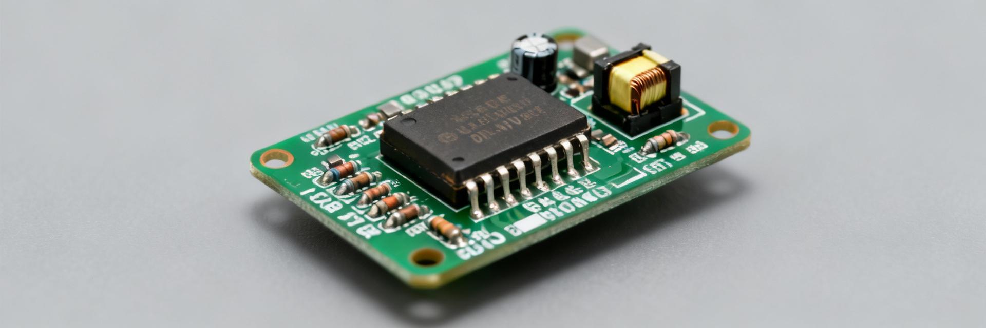
— ACPL-W340-560E가 무엇인가
Point: The device is an isolated optocoupler designed for direct gate-drive use; Evidence: manufacturer datasheet lists reinforced isolation at ~5600 Vrms and peak output current around 1.0 A; Explanation: that combination makes the part suitable where galvanic separation and short-duration drive pulses are required while keeping the drive circuitry compact and board-mountable.
— When to pick this part vs. a standard driver
Point: Choose this part when isolation and modest peak drive matter more than sub-nanosecond timing; Evidence: propagation and rise/fall timing in the datasheet imply practical PWM operation up to mid-hundreds of kHz with proper resistor choices; Explanation: if your design needs reinforced isolation, short gate-charge bursts (hundreds of mA–1 A) and a compact footprint, this part fits; for multi-amp continuous drive or very high-frequency switching, consider dedicated isolated gate-driver ICs and validate using the datasheet curves.
— Datasheet deep-dive: static & DC electrical characteristics (data analysis)
— Input LED and input-side parameters
포인트: 입력 LED 사양을 MCU/논리 드라이브용 저항기로 변환합니다. 증거: 일반적인 LED 전방 전압은 ~1.2V이며 권장 LED 드라이브 범위는 데이터시트당 5-20mA의 중심에 있는 경우가 많습니다. 설명: 3.3V MCU 핀 및 대상 IF = 10mA, R = (3.3V 1.2V) / 10mA 210. 항상 데이터시트의 입력 CTR/전송 또는 권장 LED 전류를 확인하고 높은 주변 온도에서 지속적인 작동을 위해 감쇠하십시오
- 출력 단계: 전류 기능, 전압 스윙 및 DC 한계
점: 게이트 충전 요구에 DC 출력 사양을 지도합니다;증거: 출력은 공급 레일에 가까운 보장된 논리 수준 전압을 가진 1 A 근처의 피크 출증증거 증증거 증거 증거 증거 증거 증거 증거 증거 증거 증거 증거 증거 증거설명: 효과적인 게이트 용량 Cg = 1,000 pF를 가진 MOSFET의 경우 ΔV = 15 V를 통해 전환, 게이트 충전 Q ≈ Cg·ΔV = 15 nC. 100 ns에서 그 충전을 이동하려면 I = Q / t = 15 nC / 100 ns = 0.15 A 피크가 필요합니다.데이터시트 절대 최대 값을 사용하여 연속 vs 연연연동 작업부하를 크기화합니다.use the data sheet absolute maximums to size continuous vs pulsed workloads.
작은 CSS 막대 시각화(인라인 스타일은 값을 나타냄)— Gate driver dynamic performance & switching specs (data analysis / gate driver)
— Timing: propagation delay, rise/fall time, and jitter
포인트: 타이밍 수치는 데드 타임 및 동기화 전략을 결정합니다. 증거: 데이터시트의 일반적인 전파 지연 수치는 마이크로 초 또는 마이크로 초 미만이며 상승/하강 시간은 수십 ~ 수백 나노초 범위로 제공됩니다. 설명: FPGA/MCU 데드 타임을 설정할 때 전환당 예산 1개의 전파 지연과 2개의 상승/하강 창이 제공됩니다. 예: tpd 1 s 및 tr 50 ns인 경우 데드 타임 1.1 s + 마진을 설정합니다. 실제 부하에서 입력 대 출력 지연의 벤치 캡
- 동적 전류 기능 및 전환 파형 동작
포인트: 증거: 데이터 시트 동적 곡선은 낮은 듀티 사이클에서 허용되는 피크 전류를 나타내고 펄스 폭/온도로 디레이트한다; Evidence: dataset dynamic curves shows permissive peak curs at low duty cycles and derating with pulse width / temperature; 설명: 출력 전류 대 시간 그래프를 사용하여 안전한 펄스 폭을 계산하기 위해 예를 들어, 1A 피크에서 장치는 높은 반복률에서만 마이크로초 스케일 펄스를 허용할 수 있다; 데이터 시트에 제공된 펄스당 열 에너지 및 열 시간 상수로부터 허용 듀티 사이클을 도출합니다.
작은 시각적 "펄스 폭 vs 허용 피크" 모의실험— Application design & PCB implementation (method / how-to)
- 권장 트 드라이브 회로 토폴로지 및 구성 요소 선택
포인트: 직렬 트 저항기와 적절한 디커플링이 있는 단일 엔드 트 드라이브 도식을 사용합니다. 증거: 데이터시트 절대 최대값은 공급 핀과 트 소스 허용오차를 정의합니다. 설명: 속도 대 오버슈트를 거래하기 위해 트 저항기 Rg를 선택합니다. 드라이브 레일 VDD = 15V 및 원하는 피크 Ipk 1A, Rg VDD / Ipk = 15. 더 빠른 가장자리와 더 높은 Ipk를 사용하는 경우 Rg를 줄이지만 범위로 링잉 및 VGS 오버슈트를 확인합니다. 큰 트 충전 또는
- PCB 레이아웃, 격리 및 열/크립 페이지 모범 사례
포인트: 레이아웃 선택은 격리를 보존하고 기생충을 최소화합니다. 증거: 지정된 Vrms에 대한 datasheet-recommended 크리프 및 일반 격리 관행은 몇 밀리미터의 간극 및 분리 리턴 평면을 요구합니다. 설명: 입력 및 출력 접지를 분리하고, 공급 핀에서 2-3mm 이내에 바이패스 캡을 배치하고, 고전류 루프를 짧고 넓게 이동하며, 나열된 격리 레벨에 대해 8-12mm의 목표 크리프 거리를 지정합니다. 최악의 경우 전환 시 패키지 온도 상승을 측정하여 접합 한계를 초과하지
— 사용 사례, 테스트 및 검증 (사례 연구 + 벤치)
— Typical application examples & where this device excels
Point: The device excels in medium-voltage isolated gate drive and isolated PWM outputs; Evidence: reinforced isolation and short-pulse drive capability match inverter-leg and industrial converter needs; Explanation: examples include half-bridge gate isolation in motor drives where isolation voltage and brief 1 A drive pulses are required, and isolated PWM for industrial I/O. For each, key datasheet parameters are isolation rating, peak output current, propagation delay, and thermal limits.
— Bench tests to validate datasheet claims
Point: Run a short checklist of measurements to confirm real-world behaviour; Evidence: datasheet gives test conditions to reproduce—input current, supply rails, and load conditions; Explanation: suggested tests: (1) measure propagation delay with a pulse generator and scope (100 MHz+ bandwidth, 10× probes), (2) capture rise/fall under a calibrated gate load (e.g., 1 nF), (3) deliver controlled current pulses to verify peak capability and thermal response, and (4) perform isolation withstand tests per the datasheet conditions using certified equipment. Acceptable variance: typical figures ±20% vs datasheet typical, always below datasheet maximums.
small interactive checklist badge— 생산 (행동)을 위한 문제 해결 및 실용적 체크리스트
-일반적인 장애 모드 및 수정
요점: 고장은 일반적으로 레이아웃 또는 스트레스와 관련이 있습니다. 증거: 생산에서 볼 수 있는 일반적인 문제는 낮은 Rg, 누락된 디커플링으로 인한 공급 불안정성 및 반복된 고에너지 펄스로 인한 열 과다 스트레스입니다. 설명: - Rg를 5-20 단계로 올려 링을 길들이고, 장치 전원 핀의 2-3mm 이내에 0.1F 디커플링을 추가 또는 재배치하고, 펄스 듀티 사이클을 줄이거나 열 싱크를 추가합니다. 실패한 장치의 경우 트 저항기 값
- 사전 제작 및 규정 준수 체크리스트
Point: A concise verification list prevents costly recalls; Evidence: datasheet absolute maximums and test conditions drive the checklist; Explanation: before volume: confirm input resistor sizing and LED current, verify propagation delay and rise/fall under target load, perform isolation withstand per datasheet, ensure layout creepage/clearance targets, and validate thermal performance under worst-case switching. Keep test records aligned with the manufacturer datasheet test conditions for compliance.
small inline table-like block (responsive)- 키 요약
인라인 요소를 통해 마커 모양이 조정된 사용자 지정 스타일 목록-
The device combines reinforced isolation and short-pulse 1 A output capability, making it suitable for isolated gate-drive roles in medium-power converters; sizing gate resistors and timing per datasheet ensures robust operation.
-
Translate LED Vf and desired IF into a resistor: example 3.3 V MCU, IF=10 mA → ~210 Ω; always verify with the datasheet input curve.
-
For a 1,000 pF gate at 15 V, Q ≈ 15 nC; to switch in 100 ns needs ~0.15 A peak, under the device's short-pulse capability—use datasheet dynamic curves to set pulse widths.
— Common questions and answers
Accordion using details/summary (semantic for SEO and accessible), styled inline장치에서 전달 지연 및 타이밍을 확인하려면 어떻게 해야 합니까?
프로토타입에서 어떤 트 저항기 값으로 시작해야 합니까?
생산 전에 격리를 어떻게 테스트해야 합니까?
Conclusion / Summary
Reading theACPL-W340-560Edatasheet with a focus on input LED constraints, output peak-current windows, timing budgets, and thermal derating allows engineers to size resistors, set FPGA/MCU dead-time reliably, and lay out PCBs for safe operation. Practical next step: on your first prototype, run the input-to-output propagation delay test under the targeted gate load and temperature to validate timing margins before scaling to production.
