この記事では、公表された仕様とベンチ測定を比較します。0 420 CDMCDS-3 R 3 MC実際のコンバータ条件下で定格3.3 uHのSMDパワーインダクタがどのように動作するかを示すために、データシートの数値を検証し、現実世界の動作を明らかにし、統合ガイダンスを提供することが目的です。テストの文脈:インダクタンス対周波数、DCR対温度、DCバイアス/飽和スイープにわたって評価された5つの同一のサンプルを使用して、現実的な期待値を設定します。
製品の背景と位置(背景の紹介)
主な公称規格一覧
ポイント:エンジニアが期待する名義値には、3.3uH ± トレタンス、典型的なDCR範囲、定格サテュレーション/DC電流およびLテスト周波数(通常100kHz)が含まれます。証拠:データシート形式の仕様は有用な出発点です。説明:インダクタンスはリップル電流を定義し、DCRは導通損失を駆動し、Isat/Irmsは回路内の余裕を設定します—それぞれがコンバーターのリップル、効率、熱設計に直接影響します。
フットプリント、マウントおよびボードレベルの考慮事項
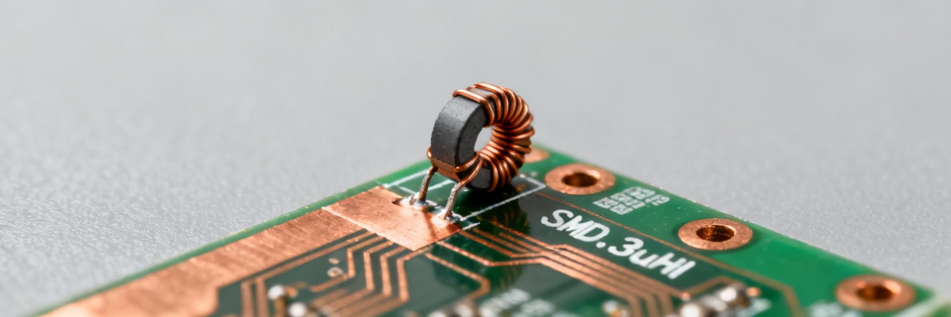
Point: The part is an SMD power inductor with a compact rectangular footprint; designers should treat it as a board-mounted power component. Evidence: Recommended land patterns and pad sizing affect solder fillet quality and thermal path. Explanation: Use a recommended PCB land pattern, add thermal copper where possible, and ensure pick-and-place tolerances and reflow profile compatibility for reliable solder joints on a small SMD 3.3uH power inductor.
データシートの仕様解説(データ分析)
Electrical spec definitions and measurement conditions
ポイント:データシートのインダクタンスは通常、小信号の測定値(例: 100 kHz、0.1 Vrms)です。証拠:データシートに記載されているLは、DCバイアスがなく、テスト周波数が定義されていることを前提としています。説明:実際には、インダクタンスは周波数とDCバイアスによって低下するため、エンジニアはLを出発点として解釈し、小信号の数値だけに頼るのではなく、負荷コンバータの動作を捉えるためにL対周波数およびL対Iを測定する必要があります。
環境および信頼性仕様の解読
ポイント:動作/保存温度、リフロープロファイル、および機械的評価は、設計マージンを提供します。証拠:熱評価は、許容される接合/周囲範囲を示します。リフローピーク温度は、はんだ付けをガイドします。説明:これらの仕様をマージンに変換してください:周囲温度が高くなるにつれて電流を減らし、クラックを避けるために推奨されるリフローに従い、アプリケーションが衝撃や振動を受けた場合には機械的マージンを許可して、長期的な信頼性を確保してください。
ベンチ測定による性能:インダクタンス、DCR、飽和(データの詳細な分析)
インダクタンスvs周波数およびDCバイアス(測定値)
Point: Measured L typically decreases with frequency and DC bias; the slope is application-critical. Evidence: Using an LCR meter and a board-mounted fixture, L measured at 100 kHz matched nominal within tolerance at zero bias, then declined under moderate DC bias. Explanation: Plot L vs F and L vs I to spot nonlinearity; if L drops significantly at expected ripple/DC bias, select a higher initial inductance or a core with better DC bias stability.
DCR, temperature rise and saturation current (measured)
Point: Four-wire DCR and thermal stabilization reveal real conduction losses and Isat behavior. Evidence: Kelvin DCR at room temp provides baseline; applying increasing DC current shows temperature rise and the point where inductance collapses (saturation). Explanation: Report DCR at room temp and at stabilized hot condition; calculate I_rms heating and compare to rated Irms to predict in-circuit temperature and performance degradation under load.
Test methodology & reproducible measurement setup (method guide)
Recommended lab setup and fixtures
要点:再現可能なテストセットアップは寄生を最小限に抑え、比較可能なデータを提供します。証拠:精密LCRメーター、校正済み治具、またはケルビンパッド付きの短いPCBトレース、精密電流源、熱電対/赤外線カメラを用いて熱マッピングを行う。説明:リードの長さを最小限に抑え、器具をゼロにし、器具の寄生を記録することで、他のエンジニアがL対FやDCR対Tプロットを自信を持って再現できるようにしましょう。
データ収集、不確実性および報告のベストプラクティス
ポイント:明示的な不確実性とサンプル統計により、検証が意味を持つようになります。証拠:複数のサンプル(ここでは5つ使用)をテストし、平均反復スイープを行い、標準偏差と機器の不確実性を計算します。説明: L vs F、L vs I、DCR vs Tをエラーバーとともに公開し、テスト条件(フィクスチャ、温度、測定帯域幅)を含めて、読者がデータシートからの偏差を解釈し、適切な設計マージンを適用できるようにします。
アプリケーションの影響とトレードオフ(ケースショーケース)
例:バックコンバータの波動と効率の影響
Point: Measured inductor parameters directly affect ripple current and efficiency. Evidence: For a buck running 12 V in → 1.2 V out at 1 A, fsw 500 kHz, a 3.3uH inductor yields ΔI ≈ V×D/(L×fs). Explanation: Use ΔI = (Vin−Vout)/L × D/fsw to compute ripple, then combine with measured DCR to estimate conduction loss P = I_rms^2 × DCR; small increases in DCR yield measurable efficiency loss in mid-load ranges.
When this 3.3uH SMD power inductor is a good (or poor) choice
Point: The part suits mid-frequency bucks and power filtering where size and inductance balance current capability. Evidence: Good when ripple tolerance and footprint priority outweigh lowest possible DCR. Explanation: Choose alternatives if the design needs much higher Isat, lower DCR for efficiency, or a significantly smaller footprint; weigh trade-offs between ripple, thermal rise, and regulator control-loop interactions.
Selection, PCB integration and troubleshooting checklist (actionable guidance)
Pre-selection checklist before committing to this part
ポイント:デザインロックの前に、システムの要求に対して重要な性能を確認してください。証拠:測定されたIsat vs予想されるピーク/リップル電流、DCRおよび熱制限、およびPCB過程でのはんだ/リフロー互換性を確認してください。説明:サンプルボードのクイックベンチチェックを実行してください: L vs I、動作温度でのDCR、および予想される電気および熱ストレス下でインダクタが必要に応じて動作することを確認するためのコンバータの健全性テスト。
レイアウト、はんだ付け、フィールド信頼性のヒント
ポイント:適切なレイアウトは損失を減らし、信頼性を向上させます。証拠:短い電流ループ、堅牢なグラウンドとパワーポア、およびパッド下の熱銅はホットスポットを減らします。説明:インダクタをスイッチングノードに近づけ、ループ面積を最小限に抑え、熱拡散のために銅を追加し、推奨リフロープロファイルに従い、問題が発生した場合(過剰な加熱、ノイズ)、はんだフィレット、ボードビアを検査し、L対Iを再実行して劣化部品を検出します。
要約する
この記事では、公開された仕様と再現可能なベンチ測定値を組み合わせて、エンジニアが0420CDMCDS-3R3MCin power designs. Top takeaways: measure inductance at relevant frequency and DC bias, use four-wire DCR and thermal checks, and validate saturation current in-circuit to ensure expected ripple and efficiency performance.
Key summary
-
•
Measure L vs frequency and L vs I to capture real-world behavior of the 3.3uH SMD power inductor; small-signal datasheet L is only a starting point.
-
•
四線式DCRと熱安定性を用いて熱DCRを報告し、inでの伝導損失を予測する動作電流と環境条件に傾向がある。
-
•
代表的なコンバータ設定で飽和電流を検証して、回路内のヘッドルームを確認し、DCバイアス下での予期しないインダクタンスの崩壊を回避します。
