エンジニアは引き続きACPL-W 340-560 E絶縁ゲート駆動タスクに適しています。1.0 Aのピーク出力能力と5600 Vrmsのデータシート指定の絶縁耐定格と組み合わせて、予測可能な絶縁と中電力インバータの駆動を実現します。この記事では、これらの見出しの数字を使用して、実用的なデータシートの解釈、ゲートドライバのタイミングと電流バジェット、PCB/サーマルレイアウトの実践、実世界の行動を検証するコンパクトなベンチテストチェックリストです
-クイック背景と主要仕様(背景の紹介))))))。
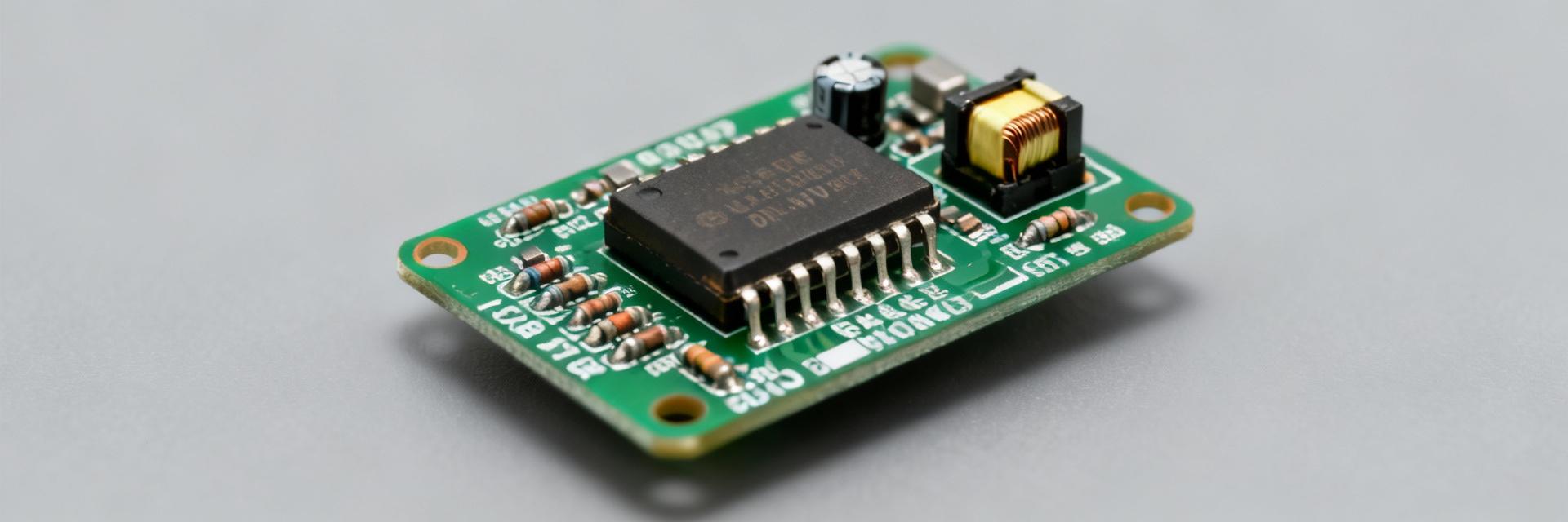
-ACPL-W 340-560 Eとは何ですか?
Point: The device is an isolated optocoupler designed for direct gate-drive use; Evidence: manufacturer datasheet lists reinforced isolation at ~5600 Vrms and peak output current around 1.0 A; Explanation: that combination makes the part suitable where galvanic separation and short-duration drive pulses are required while keeping the drive circuitry compact and board-mountable.
— When to pick this part vs. a standard driver
Point: Choose this part when isolation and modest peak drive matter more than sub-nanosecond timing; Evidence: propagation and rise/fall timing in the datasheet imply practical PWM operation up to mid-hundreds of kHz with proper resistor choices; Explanation: if your design needs reinforced isolation, short gate-charge bursts (hundreds of mA–1 A) and a compact footprint, this part fits; for multi-amp continuous drive or very high-frequency switching, consider dedicated isolated gate-driver ICs and validate using the datasheet curves.
— Datasheet deep-dive: static & DC electrical characteristics (data analysis)
— Input LED and input-side parameters
ポイント:入力LED仕様をMCU/ロジックドライブ用の抵抗に変換します。証拠:典型的なLEDの順方向電圧は約1.2 Vであり、推奨されるLEDドライブ範囲は、データシートによるとしばしば5ー20 mAの中心にあります。説明: 3.3 V MCUピンとターゲットIF=10 mAの場合、R=(3.3 V-1.2 V)/10 mA≈210Ω。常にデータシートの入力CTR/転送または推奨されるLED電流とディレーティングを確認して、周囲温度が高い状態で持続的に動作するようにしてください。
-出力ステージ:電流能力、電圧スイング、およびDC制限
ポイント: DC出力仕様をゲート充電ニーズにマッピングします。証拠:出力は、電源レールに近いロジックレベルの電圧が保証された1 A近くのピークパルスに対して指定されています。説明:ΔV=15 Vにわたる有効ゲート容量Cg=1,000 pFスイッチングを持つMOS FETの場合、ゲート充電Q≈Cg·ΔV=15 nC。その充電を100 nsで移動するには、I=Q/t=15 nC/100 ns=0.15 Aピークが必要であり、短いパルスの1 Aピーク能力を大幅に下回ります。データシートの絶対最大値を使用して、連続対パルスのワークロードを体格してください。
小さなCSSバーの視覚化(インラインスタイルは値を表します)— Gate driver dynamic performance & switching specs (data analysis / gate driver)
— Timing: propagation delay, rise/fall time, and jitter
ポイント:タイミングの数字はデッドタイムと同期戦略を決定します。証拠:データシート上の典型的な伝搬遅延の数字はマイクロ秒またはサブマイクロ秒のスケールであり、立ち上がり/立ち下がり時間は数十ー数百ナノ秒の範囲で与えられます。説明: FPGA/MCUのデッドタイムを設定する際に、遷移ごとに1つの伝搬遅延と2つの立ち上がり/立ち下がりウィンドウを予算化します。例:tpd≈1μs、tr≈50 nsの場合、デッドタイム≥1.1μsプラスマージンを設定します。ジッターと最悪の遅延をキャプチャするために、実際の負荷下での入出力遅延のベンチキャプチャで確認してください。
-動的な電流能力とスイッチング波形の振る舞い
ポイント: dV/dtイベント中の短い高電流パルスは許容されますが、熱的に制限されます。証拠:データシートの動的曲線は、低デューティサイクルで許容ピーク電流を示し、パルス幅/温度によって減衰します。説明:出力電流対時間グラフを使用して安全なパルス幅を計算します。たとえば、1 Aピークでは、デバイスは高繰り返しレートでマイクロ秒スケールのパルスのみを許容する可能性があります。
小さな視覚的な「パルス幅と許容ピーク」モックアップ— Application design & PCB implementation (method / how-to)
— 推奨ゲートドライブ回路トポロジーおよび部品の選択
ポイント:直列ゲート抵抗と適切なデカップリングを備えたシングルエンドゲートドライブ回路図を使用してください。証拠:データシートの絶対最大値は、電源ピンとゲートソースの公差を定義します。説明:速度とオーバーシュートを交換するためにゲート抵抗Rgを選択してください:ドライブレールVDD=15 V、所望のピークIpk≤1 A、Rg≥VDD/Ipk=15Ω。より速いエッジとより高いIpkを受け入れる場合は、Rgを減らしますが、リンギングとVGSオーバーシュートをスコープで確認してください。大きなゲート充電または長いケーブルランを駆動する場合は、クランプ/スナバとブリーダー抵抗を含めてください。
–PCBレイアウト、絶縁、熱/クリープのベストプラクティス
ポイント:レイアウトの選択によって絶縁が保たれ、寄生虫が最小限に抑えられます。証拠:指定されたVrmsのdatasheet-recommendedい沿面と一般的な絶縁の実践には、数ミリメートルのクリアランスと分離されたリターンプレーンが必要です。説明:入力と出力のグラウンドを分離し、バイパスキャップを供給ピンから2ー3 mm以内に配置し、高電流ループを短く広く配線し、リストされた絶縁レベルの目標沿面距離を8ー12 mmに設定します。最悪の場合のスイッチングでパッケージ温度上昇を測定して、ジャンクション制限を超えないように熱挙動を検証します。
-ユースケース、テスト、検証(ケーススタディ+ベンチ)
— Typical application examples & where this device excels
Point: The device excels in medium-voltage isolated gate drive and isolated PWM outputs; Evidence: reinforced isolation and short-pulse drive capability match inverter-leg and industrial converter needs; Explanation: examples include half-bridge gate isolation in motor drives where isolation voltage and brief 1 A drive pulses are required, and isolated PWM for industrial I/O. For each, key datasheet parameters are isolation rating, peak output current, propagation delay, and thermal limits.
— Bench tests to validate datasheet claims
Point: Run a short checklist of measurements to confirm real-world behaviour; Evidence: datasheet gives test conditions to reproduce—input current, supply rails, and load conditions; Explanation: suggested tests: (1) measure propagation delay with a pulse generator and scope (100 MHz+ bandwidth, 10× probes), (2) capture rise/fall under a calibrated gate load (e.g., 1 nF), (3) deliver controlled current pulses to verify peak capability and thermal response, and (4) perform isolation withstand tests per the datasheet conditions using certified equipment. Acceptable variance: typical figures ±20% vs datasheet typical, always below datasheet maximums.
small interactive checklist badge-生産のためのトラブルシューティングと実践的なチェックリスト(アクション)
-一般的な障害モードと修正
ポイント:故障は通常、レイアウトまたはストレスに関連しています。証拠:生産で見られる典型的な問題には、低Rgからのリンギング、欠落したデカップリングによる供給不安定性、および高エネルギーパルスの繰り返しによる熱過負荷があります。説明:修正-リンギングを抑えるためにRgを5ー20Ωステップで上げる、デバイス電源ピンから2ー3 mm以内に0.1μFのデカップリングを追加または再配置する、パルスデューティサイクルを減らす、またはヒートシンクを追加する。故障したユニットの場合、ゲート抵抗値、デカップリング配置を確認し、負荷下でパッケージ温度を測定してください。
-プリプロダクションとコンプライアンスのチェックリスト
Point: A concise verification list prevents costly recalls; Evidence: datasheet absolute maximums and test conditions drive the checklist; Explanation: before volume: confirm input resistor sizing and LED current, verify propagation delay and rise/fall under target load, perform isolation withstand per datasheet, ensure layout creepage/clearance targets, and validate thermal performance under worst-case switching. Keep test records aligned with the manufacturer datasheet test conditions for compliance.
small inline table-like block (responsive)-キーサマリー
インライン要素を使用してマーカーの外観を調整したカスタムスタイルのリスト-
The device combines reinforced isolation and short-pulse 1 A output capability, making it suitable for isolated gate-drive roles in medium-power converters; sizing gate resistors and timing per datasheet ensures robust operation.
-
Translate LED Vf and desired IF into a resistor: example 3.3 V MCU, IF=10 mA → ~210 Ω; always verify with the datasheet input curve.
-
For a 1,000 pF gate at 15 V, Q ≈ 15 nC; to switch in 100 ns needs ~0.15 A peak, under the device's short-pulse capability—use datasheet dynamic curves to set pulse widths.
— Common questions and answers
Accordion using details/summary (semantic for SEO and accessible), styled inlineデバイスの伝搬遅延とタイミングを確認するにはどうすればよいですか?
プロトタイプではどのゲート抵抗値から始めるべきですか?
本番前にアイソレーションをどのようにテストすればよいですか?
結論 / 摘要
読んでいるACPL-W340-560E入力LEDの制約、出力ピーク電流窓、タイミング予算、および熱劣化に焦点を当てたデータシートは、エンジニアが抵抗を設計し、FPGA/MCUのデッドタイムを確実に設定し、安全な運用のためのPCBレイアウトを行うことを可能にします。実用的な次のステップ:最初のプロトタイプでは、ターゲットゲート負荷と温度下で入力から出力の伝播遅延テストを実行し、スケールアップに向けて前にタイミングマージンを検証します。
