Introduction: A concise datasheet snapshot: the 046882130099846+ family is presented in a compact surface-mount package with a multi-pin interface, nominal primary supply range suitable for low-voltage systems, and a peak current class designed for moderate-load applications; a standout feature is integrated sequencing/enabling behavior that affects power-up margins. This article translates the raw datasheet into actionable design guidance, verification steps, and a checklist for confident design-in, focusing on clear pin mapping, electrical-spec highlights, test procedures, integration notes, and troubleshooting.
Background & Quick Part Overview
What this part is and typical applications
Point: This device is a multi-function connector/IC-class component intended for board-level signal/power interfacing in compact electronics. Evidence: The datasheet front page classifies the device by package and intended use, noting target markets such as portable systems and compact modules. Explanation: Designers choose this part for space-constrained boards where combined signal and power routing, predictable enable behavior, and a small thermal footprint matter; typical applications include sensor hubs, small communication modules, and mobile peripherals.
How to locate the authoritative datasheet pages
Point: Confirming you have the correct datasheet revision prevents costly mistakes. Evidence: Key identifiers on the datasheet include full part number variant (046882130099846+ suffices as family), revision or document code, ordering suffixes, and packaging codes. Explanation: Check the revision history and errata section for last-minute clarifications; verify ordering suffixes against your BOM, and match package codes to your PCB footprint to avoid mismatches in assembly and performance.
Pinout & Physical Layout
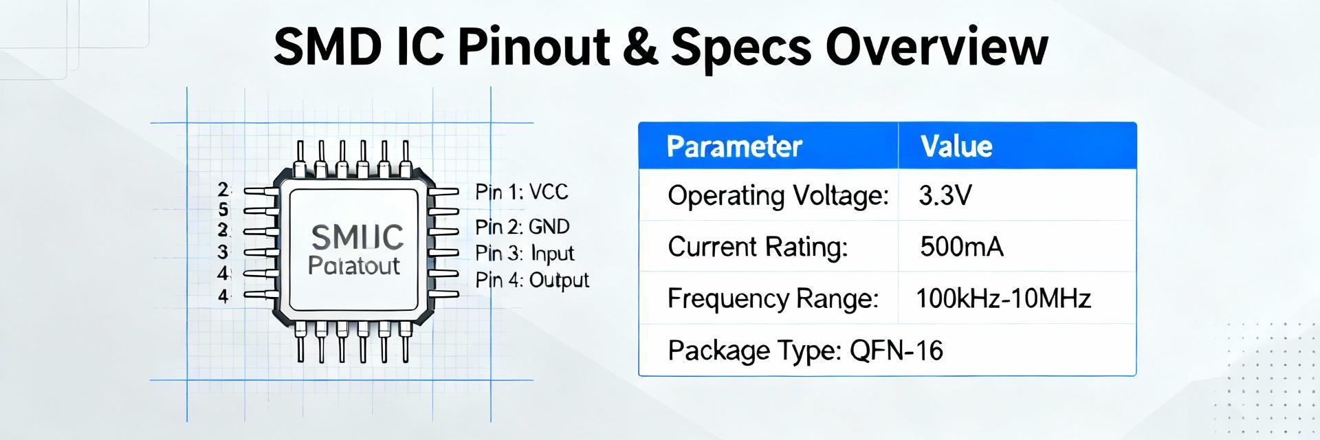
Pin mapping: role-by-pin
A precise pinout table is the first verification step for layout and wiring. Designers must flag power pins, dedicated grounds, and control signals.
Package drawing, footprint and mechanical notes
Mechanical compatibility is as critical as electrical. Verify units (mm vs. mil), tolerances, and recommended solder fillet sizes; ensure the footprint includes required courtyard and keepout areas. For thermal pads, follow pad size and via recommendations and confirm solder mask openings to achieve reliable wetting and reflow consistency.
Electrical Specifications Deep‑Dive
Operating Range Visualizer
Absolute maximum ratings
Absolute maximums define immediate failure thresholds. Extract the worst-case absolute values and then derate for system margin. Present these as a short quick-reference table on your design checklist and call out any pins with asymmetric limits or latch-up susceptibilities.
DC/AC characteristics and power budgets
Prioritize DC logic thresholds, I/O drive, and power dissipation rows. Use timing diagrams to compute worst-case setup/hold margins; combine dynamic current figures with switching frequencies to estimate average and peak power. Summarize the must-know specs for system engineers in a compact table for quick reference during integration.
How to Verify & Test Claims
Practical lab checks: Lab validation confirms real-world behavior against the datasheet. Use a calibrated bench PSU with current measurement and a scope with adequate bandwidth. Record conditions (ambient, VIN, load type) and compare against datasheet “typical” and “max” rows.
Red flags: Spotting inconsistencies early saves time. Common issues include mismatches between schematic pins and pin table, or missing thermal resistance data.
Integration Case Study
Layout Highlights: Place decouplers (
Thermal: Estimate junction temperature by summing ambient plus (power dissipation × thermal resistance). Increase copper area if temperature approaches recommended limits.
Practical Action Checklist & Troubleshooting
Pre-production Checklist
- ✔ Verify pinout vs. footprint
- ✔ Confirm supply sequencing
- ✔ Implement recommended decoupling
- ✔ Validate absolute max margins
Common Failure Modes
- ✘ No Power: check VIN/GND continuity
- ✘ Comm Errors: verify pull-up resistors
- ✘ Overheating: check thermal via count
Summary
- Use the datasheet to extract the authoritative pinout and populate a verified pin table before layout; pay special attention to power, ground, and enable pins.
- Prioritize absolute maximums and recommended operating conditions; derate operating points and include thermal margin calculations.
- Implement lab validation steps: static supply current, logic thresholds, and timing under realistic loads.
- Follow a pre-production checklist that includes footprint verification and supply sequencing to reduce field failures.
