Designers need concrete, measured rules for reliable 10-pin 0.5mm FPC assembly. Industry benchmarks for 0.5 mm FPC land patterns typically fall within 0.18–0.30 mm for pad width and 0.6–1.0 mm for pad length, with stencil paste coverage commonly targeted at 60–80%. This guide delivers exact PCB pad recommendations, footprint rules, and measurable footprint benchmarks to use directly in CAD and pilot-run validation.
Background: Connector Basics and Footprint Constraints
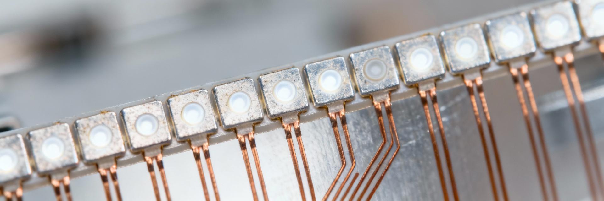
Why Pitch, Pad Shape, and Plating Matter
At 0.5 mm pitch, pad geometry directly drives solder volume and bridging risk. Tighter pitch reduces allowable pad-to-pad clearance and increases wetting interaction, making PCB pad shape and mask definition critical. Rectangular pads provide more solder volume; rounded or tapered pads reduce bridging—choose based on solder paste control and whether NSMD or SMD pads are specified.
Mechanical vs Electrical Requirements
Footprint design must satisfy mechanical insertion, latching, and electrical contact consistency. Contact length and mating tolerance determine required pad land length and keepout zones; low-speed signals rarely require controlled impedance. Include pin-to-pin clearance, connector alignment fiducials, and physical keepouts as non-negotiable items on the mechanical drawing.
Core Specification Benchmarks
Benchmark Pad Dimensions & Layout Recipes
Recommended Pad Geometry (Conservative vs. Compact)
Provide two practical pad recipes so designers can choose risk vs. density. Conservative pads favor hand/reflow robustness; compact pads favor high-density automated assembly. Use the conservative recipe for first articles and fragile assemblies, move to compact once stencil/paste and placement are validated for yield.
Conservative Recipe
- •Pad Width: 0.28 mm
- •Pad Length: 0.90 mm
- •Pitch: 0.50 mm
- •Solder Mask: Pad + 0.05 mm
Compact Recipe
- •Pad Width: 0.20 mm
- •Pad Length: 0.70 mm
- •Pitch: 0.50 mm
- •Solder Mask: Pad + 0.00 to -0.02 mm
Stencil Apertures and Paste Coverage Benchmarks
Stencil aperture and paste volume control bridging and wetting. For 0.5 mm pitch, recommended paste coverage is 60–80% of pad area with rectangular or tapered apertures to aid release. Start with 70% coverage; measure paste transfer efficiency and adjust aperture shape to hit paste volume targets without increasing bridging.
Manufacturing and DRC Rules to Enforce in PCB CAD
Layer Stack & Finish
Copper thickness and surface finish affect solder wetting. Heavier copper retains more heat and can change wetting dynamics; finishes with higher wettability reduce required solder volume. Specify the copper weight and finish early; design minimum annular rings and clearances with the chosen finish in mind.
Assembly, Reflow and Inspection Benchmarks
Reflow Profile Controls
Short leads and small pads benefit from controlled soak to prevent tombstoning. Use a moderate ramp (0.8–1.5 °C/sec), a brief soak to equalize board temperature, and a peak within the paste supplier range. Add AOI rules focusing on fillet and bridging.
Acceptance Metrics
Useful metrics include bridging rate, contact continuity, and insertion force consistency. Set targets (e.g., bridging incidence
Summary & Recommendations
Main Recommendation: Use conservative pad set (0.28mm width, 0.90mm length) for first articles. Transition to compact set only after validating paste transfer.
Stencil Target: Aim for 60–80% coverage. Monitor paste volume variation (
Process Tracking: Log bridging rate, contact continuity, and insertion force. Validate with a 1–5 board pilot run before full production.
