Accurate interpretation of the 045971-4185 connector datasheet, correct pinout mapping, and a verified PCB footprint are the highest-impact actions to prevent PCB assembly failures and rework. This practical, data-led reference provides critical datasheet insights, reliable pin mapping, and manufacturable PCB footprint derivations.
Overview: Key Specifications and Background
The 045971-4185 connector is a compact wire-to-board interconnect designed for mixed-signal, low-voltage applications requiring a small pitch and low-profile mating. It is ideally suited for board-level connections between subassemblies, cable harnesses, or daughtercards where controlled mating cycles and precise current ratings are vital for system reliability.
Quick Specification Snapshot
| Parameter | Value (Example) | Notes for Footprint Design |
|---|---|---|
| Part Type | Wire-to-board | Determines mating orientation & retention features |
| Contact Count | 8 Contacts | Defines pad array size and placement |
| Pitch | 1.27 mm | Drives pad-to-pad spacing & soldermask relief |
| Rated Current/Voltage | 1.5 A / 50 V | Influences trace width & thermal relief |
| Operating Temp | -40°C to +105°C | Material selection & solder process window |
Use Cases: When to Choose This Connector
This connector is optimal for board-stacking or compact cable interconnects requiring a low profile and modest current ratings. It fits constrained form factors where pitch limits routing density. Decision Cues: If current per contact is less than 2A and mating cycles are between 500 and 1,000, this component is appropriate for signal and low-power rails.
Datasheet Deep Dive: Critical Parameters
Extracting dimensions, tolerances, and electrical specs is the first step in mapping design rules. Use the datasheet to create a checklist: mechanical drawings first, followed by electrical ratings and reliability data.
Mechanical Tolerances
Extract pad-to-pad centerlines and keep-out areas. If a tolerance of ±0.1 mm is listed, apply a ±0.15 mm margin in your DRC for initial prototypes.
Electrical & Reliability
Map ampacity to copper pour strategy. Use voltage ratings to set creepage and clearance constraints for your PCB layout.
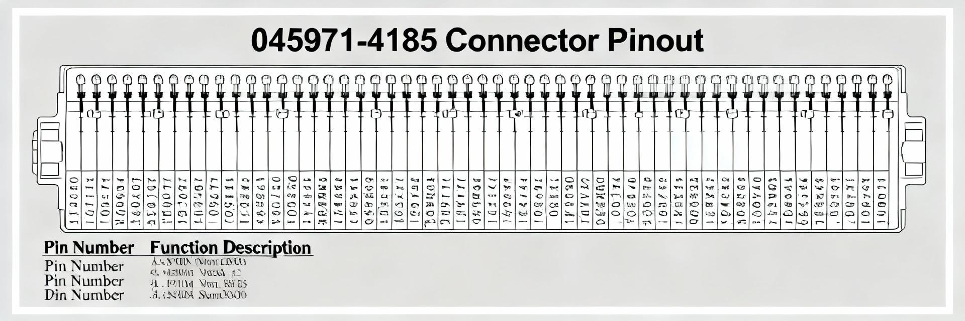
Pinout Mapping & Schematic Guidance
Accurate pin mapping prevents swapped nets. Establish the manufacturer datum and mating face to create a clear pin-to-signal table.
| Pin # | Signal Name | Function | Recommended Net Type | Test Point? |
|---|---|---|---|---|
| 1 | VIN (Example) | Power Input | Power | Yes |
| 2 | GND | Return | Ground | No |
| 3 | SIG1 (Example) | Data | Signal | Optional |
PCB Footprint & Land Pattern
Derive the footprint from mechanical dimensions. Ensure pad length and width accommodate a reliable solder fillet, and soldermask openings are sized to control wetting.
Practical Implementation & Testing
Assembly Considerations
- • Ensure solder profile matches thermal limits.
- • Use mechanical support for high-mating-force parts.
- • Inspect fillet quality and alignment marks.
Validation Checklist
✓ Continuity and pin-to-pin mapping
✓ Insulation resistance > 100 MΩ
✓ Contact resistance
✓ Mechanical retention (pull test)
Summary
Designing with the 045971-4185 connector requires meticulous attention to datasheet dimensions to mitigate assembly risks. By extracting precise tolerances and validating pinouts early, engineers ensure long-term reliability.
- Verify critical dimensions and tolerances before drawing pads.
- Generate a 3D STEP model and run DRC/DFM checks.
- Close the loop with a one-off assembly test and retention check.
