0452003.MRL Data Sheet Deep Dive: Specs & Footprint
In modern PCB designs, a large share of late-stage board respins and field failures trace back to mismatched component specs or incorrect land patterns. This deep dive explains which electrical and mechanical parameters designers must lock down to avoid costly mistakes and rework.
The article unpacks electrical specs, thermal and reliability limits, and provides a ready-to-use footprint and land-pattern checklist for PCB layout. Readers will get quick-reference tables, measurement/verification steps, and copy-ready checklist lines to paste into CAD libraries and BOM notes.
Product Overview & Key Specs
What the 0452003.MRL is
The 0452003.MRL is a slow-blow surface-mount time-delay fuse sized for board-level circuit protection, rated for low- to moderate-current protection where controlled inrush or short-duration overloads occur.
- •Point: Surface-mount time-delay protection.
- •Evidence: Nominal current and AC/DC voltage ratings define its class.
- •Action: Synchronize CAD library values with manufacturer data.
Spec highlights at a glance
| Parameter | Typical Value |
|---|---|
| Rated current | 3 A |
| Rated voltage | 125 VAC / 125 VDC |
| Interrupt rating (IR) | 35 A @ specified voltage |
| Package / Series | Nano 2 / 452 family |
| Typical I²t | See Time-Current Curve |
Electrical Performance & Thermal Limits
Time-current characteristic & inrush behavior
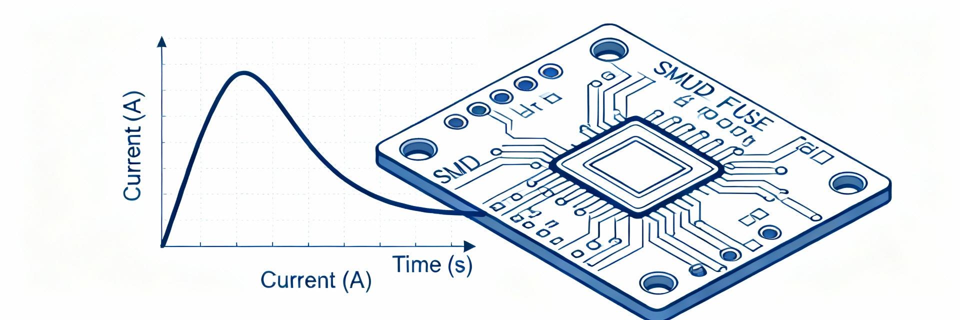
The time-current curve defines how long the fuse tolerates overcurrent before opening. Slow-blow curves are specifically engineered to allow large short-duration inrush currents typical of motors or capacitor banks. By comparing the expected inrush I²t to the fuse curve, designers can predict margin and ensure reliability.
Action: Compute worst-case inrush I²t and plot it against the fuse curve captioned "0452003.MRL time-current curve" for verification.
Rated voltage, interrupt rating, and derating
Rated AC/DC voltage sets the maximum safe operating system voltage, while the interrupt rating (IR) limits the safe clearing of fault currents. High ambient temperatures or dense PCB spacing reduces thermal margin.
Typical derating rule: Reduce rated current by 10%–20% for elevated ambient temperatures.
Mechanical Dimensions & Footprint Requirements
Exact mechanical dimensions
Critical dimensions include overall length, width, height, and lead/pad center distances. Use the overall body outline as a keepout zone and pad center spacing for electrical clearance.
PCB land pattern & stencil guidance
Correct pad sizes and stencil apertures determine solder joint reliability. Use slightly elongated pads for easier inspection or hand soldering, and 60%–80% aperture for stencils.
Implementation Note:
Specify "0452003.MRL PCB land pattern" in fabrication notes to ensure assembly accuracy.
Assembly, Soldering & Reliability Considerations
Soldering Profile & Limits
Exceeding peak temperature or time-above-liquidus leads to internal element degradation. Hand-soldering should avoid direct heating of the fuse body.
Environmental Testing
Thermal cycling, humidity, and vibration tests reveal latent failures. Watch for increased resistance (ΔR) or intermittent opens after stress tests.
- Thermal Shock Resistance
- Humidity Soak Tolerance
- Mechanical Vibration Resilience
Comparison & Selection Tips
When to choose this part vs. close alternatives
Selection hinges on current margin, IR needs, and inrush tolerance. Choose this slow-blow compact fuse when inrush pulses are expected and moderate IR suffices. If fault currents exceed 35A, consider a larger case size or higher IR variant.
*Always annotate reel vs. cut-tape in BOM.
Quick Checklist & Implementation Steps
Pre-layout (CAD Preparation)
- Confirm continuous/interrupting current ratings.
- Reserve keepout and thermal relief zones.
- Set pad finish and SMD orientation.
- Validate stencil aperture & mask clearances.
- Document mechanical hold-downs for vibration.
Post-layout (Validation)
- Run solderability samples on prototypes.
- Perform functional inrush tests with probes.
- Thermal imaging to detect hotspots.
- Visual solder-fillet inspection (first-article).
- Verify ΔR resistance stays within limits.
Key Summary
- Verify Electrical Limits: Ensure interrupt rating and continuous rating have adequate margin to avoid nuisance opens.
- Optimize Footprint: Correct pad sizing and mask clearance are essential for reliable solder fillets.
- Two-Step Validation: Use the pre-layout checklist for design and post-layout testing for assembly verification.
