Comprehensive technical insights into high-density protection for modern IoT and portable electronics.
Modern portable and IoT designs are driving higher current density into ever-smaller PCB real estate, pushing designers toward compact protection devices. Industry sampling shows more boards placing Polyfuses and fast-acting chip fuses on sub-2 mm footprints; the SMD fuse 0603 is a frequent choice where designers need ~1–2 A protection while preserving space.
This guide focuses on how a 1.75A rated device behaves electrically and how to implement a reliable PCB footprint and layout, bridging the gap between datasheet specs and real-world assembly.
Why the SMD fuse 0603 is common for compact power protection
Typical use cases and system-level tradeoffs
Typical products include wearables, compact sensors, and small power-rail modules. These systems share tight area budgets and often need single-digit-amp protection. Choosing a 1.75A fuse trades thermal mass and interrupt robustness for footprint; larger fuse bodies provide higher interrupt energy and thermal inertia, while resettable alternatives reduce one-time replacement but add resistance and size.
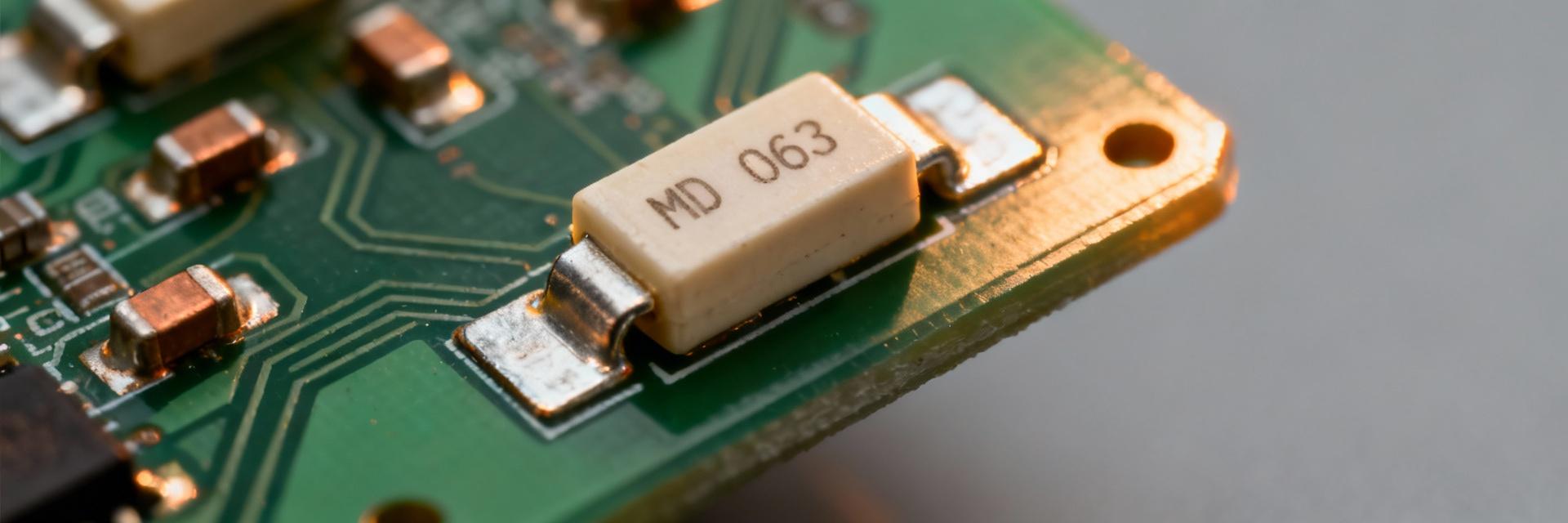
Package anatomy (1.6 × 0.8 mm)
The 0603 form factor limits thermal and mechanical margins. A 1.6 × 0.8 mm ceramic or epoxy body with plated end caps and thin internal element provides small thermal mass and limited I²t. End-cap metallurgy and termination style affect solder wetting and mechanical robustness; tight clearances demand careful pad design to ensure heat is managed and fillets form correctly during reflow.
Electrical performance metrics
Visualizing Fuse Behavior
*Representation of thermal energy capacity vs. fault energy.*
Key specs: Rated current & I²t
Reading curves is necessary when inrush or transients exist. Time-current plots demonstrate that short surges can be tolerated without nuisance open. Select a device whose time‑current curve clears true faults but survives inrush; use I²t to compare transient energy tolerance and size margin when your circuit has motors, capacitive banks, or battery connection surges.
Resistance & Derating
Series resistance governs drop and heat. DC resistance for chip fuses is small but measurable; higher resistance increases power loss at 1.75A (P = I²R). Specify max voltage rating for your rail, apply temperature derating from the datasheet for elevated board temps, and confirm interrupt rating—DC interrupt performance is usually lower than AC.
Reliability & Test Conditions
| Factor | Real-World Impact | Mitigation Strategy |
|---|---|---|
| Mounting & Reflow | Aggressive lead-free reflow can induce micro-cracks. | Follow manufacturer profiles; ensure even pad wetting. |
| Aging Effects | Resistance drift over long-term thermal cycling. | Validate long-term stability in high-temp environments. |
| PCB Copper | Acts as a heat sink, altering trip temperatures. | Use thermal reliefs to standardize dissipation. |
Designing the PCB footprint (0603)
Derive pad lands from physical body with fillet allowance. Step-by-step: base on component length/width (1.6 × 0.8 mm), allow a fillet overlap of ~0.2–0.4 mm per end, and keep a central gap matching the termination spacing.
Pad Width: 0.8 – 1.0
Gap: 0.2 – 0.4
Pad Width: 0.6 – 0.8
Gap: 0.3 – 0.4
Stencil Tip: Reduce paste apertures 10–20% per pad for reliable solder volume and to prevent bridging.
Placement and layout considerations
Thermal derating and copper pours
Maintain a minimum 0.5–1.0 mm keepout from large copper areas or include thermal reliefs; for sensitive nets, isolate the fuse pad with narrow thermal spokes so its thermal time‑constant aligns with fuse ratings. This tuning helps predictable operation during prolonged overloads.
Trace widths and vias
For sustained 1.75A, use short, wide traces; for 1 oz copper, target 1.5–3.0 mm widths depending on allowed temperature rise. Place the fuse near the power source, minimize trace length to load, and add via stitching where current must transfer between layers to reduce resistive heating.
Selection checklist before sampling
- ✔Verify rated current and time-current curve against inrush.
- ✔Confirm DC resistance and expected voltage drop at 1.75 A.
- ✔Check interrupt rating and maximum rated voltage for DC system.
- ✔Confirm operating temperature window and package tolerances.
- ✔Record preferred part code (e.g., 04381.75WR) for BOM.
Validation & test plan for prototypes
- Post-reflow visual and microscope inspection of fillets.
- Continuity and resistance verification vs. datasheet.
- Controlled overcurrent soak tests and thermal imaging.
- Mechanical shock and three-cycle thermal cycling.
- Document results and iterate pad or stencil if needed.
Summary
For compact power protection where space wins, the SMD fuse 0603 offers a practical balance for ~1–2 A rails when designers account for limited thermal mass, DC resistance, and interrupt capability. Key checks are time‑current behavior, I²t for transients, pad design for reliable fillets, and layout choices that control heat and parasitics. Prototype validation—reflow check, current soak, and imaging—should precede production to ensure consistent field performance.
- Use the 1.6 × 0.8 mm package data as the starting point for pad derivation.
- Evaluate time‑current curves and I²t to tolerate inrush while still clearing real faults.
- Keep the fuse close to the supply source and isolate large copper pours.
