This 8-position, 3.00 mm-pitch vertical PCB header is typically specified for up to 5 A per circuit with insulation considerations that can reach several hundred volts—key electrical and mechanical values you must verify before layout or replacement. This summary extracts pinout, mechanical drawings, electrical specs, thermal limits, and test tips from the manufacturer datasheet to support design decisions.
Product Overview & Key Identifiers (Background Introduction)
Part Family and Common Description
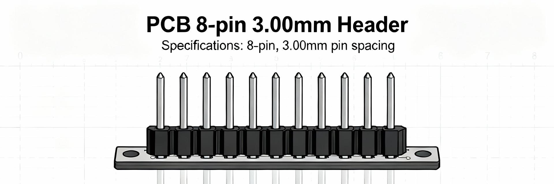
Point: The component is a single-row, 8-position vertical PCB header with 3.00 mm pitch used for board-to-board or cable headers.
Evidence: Form factor suits mixed signal and modest power distribution on control PCBs.
Explanation: Designers commonly select this header where compact vertical mating and reliable solder joints are required without full shrouding.
Part Number Deciphering
Point: Part numbers encode configuration, plating, and packaging; these affect electrical and mechanical performance.
Evidence: Typical fields include series, position count, plating finish, and packing form.
Explanation: Verify finish (tin vs. selective plating), configuration code, and any option suffixes on the manufacturer datasheet to ensure compatibility with soldering and environmental requirements.
Mechanical Specifications & Pinout (Data Analysis)
Mechanical drawings define pad layout, pin numbering, and anchor features—verify against the 0436500815 datasheet before generating footprints. Typical drawings show exact lead spacing, polarizing peg location, and recommended hole sizes. A mismatch of even 0.1 mm can cause soldering defects or mechanical interference.
Pinout Table & PCB Footprint Guidance
| Pin | Function | Plating | Recommended Hole Ø |
|---|---|---|---|
| 1 | Signal / Power | Tin | 1.20 mm |
| 2 | Signal / Power | Tin | 1.20 mm |
| ... | ... | ... | ... |
| 8 | Signal / Power | Tin | 1.20 mm |
Electrical Specifications & Performance Limits
Rated Current, Voltage, and Contact Resistance
Rated current and voltage determine safe operating envelope; designers must confirm electrical specs for application derating. Typical rating is 5 A per contact under defined temperature rise; insulation/working voltage values appear on the datasheet.
Dielectric, Insulation, and Signal Integrity
Dielectric strength and insulation resistance influence safety and performance. For mixed high-voltage and high-speed signals, add extra clearance, consider shielding, and check crosstalk/impedance only if used above low-frequency signaling.
Thermal, Environmental & Reliability Ratings
Selection, Alternatives & Application Examples
Selection Checklist
- ✔ Pitch & Position Count
- ✔ Rated Current (5A)
- ✔ Plating Type (Tin vs Gold)
- ✔ Mechanical Anchors/Pegs
Typical Applications
• Power distribution on control boards
• Sensor harness headers
• Daughtercard connectors
• Modular industrial electronics
Summary
- 1 Confirm footprint and pinout against the 0436500815 datasheet before CAD release; mismatches in pitch or peg location create assembly failures.
- 2 Verify rated current (≈5 A), insulation and dielectric test values, and apply thermal derating for elevated ambient temperatures and enclosure designs.
- 3 Use finish and mating-cycle data to select plating and environmental qualifiers; perform sample soldering and inspection to validate manufacturing process and reliability.
Frequently Asked Questions (FAQ)
Troubleshooting Checklist (Copyable)
1. Verify footprint vs. mechanical drawing.
2. Confirm hole Ø and annular ring for plating process.
3. Sample-solder 5–10 units; inspect fillets (optical/X-ray).
4. Measure contact resistance at rated current.
5. Thermal image under load for hotspots.
6. Replace headers with >20% resistance increase or visible corrosion.
