The 3.00mm, 5‑pin through‑hole header is a common choice where mixed power and signal connections meet PCB robustness requirements. This article presents a concise datasheet, clear pinout, and layout best practices for designers.
This guide promises an actionable reference: a compact spec table, explicit pin numbering rules, three example pin mappings, PCB footprint recommendations, soldering and reinforcement tips, substitution checklist, procurement notes, and troubleshooting steps to speed integration into production.
Quick Specs & Electrical Ratings
Key Electrical Specifications
Below is a compact copy/paste spec table suitable for BOMs and quick reference. Values represent typical, conservative ranges for a 5‑pin 3.00mm through‑hole header.
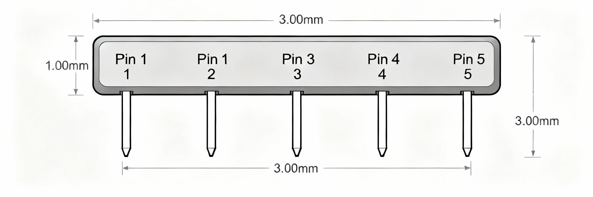
Pinout Diagram & Signal Mapping
Pin numbering typically starts at the leftmost pin when viewing the header from the component side with the shroud or notch to the top. Always verify with the mechanical drawing and silk reference on the PCB silk layer.
Example A: Serial + Power
- Pin 1: VCC
- Pin 2: GND
- Pin 3: TX
- Pin 4: RX
- Pin 5: NC
Example B: I²C + Power
- Pin 1: VCC
- Pin 2: GND
- Pin 3: SDA
- Pin 4: SCL
- Pin 5: NC
Example C: 5‑Wire Sensor
- Pin 1: VCC
- Pin 2: GND
- Pin 3: DATA
- Pin 4: CLK
- Pin 5: ALERT
Mechanical Dimensions & Footprint
Recommended PCB Land Pattern
- Drill Size: Ø1.0–1.2 mm (Plated Through-Hole)
- Pad Diameter: 1.6–2.0 mm
- Annular Ring: ≥0.5 mm
- Pitch Tolerance: ±0.10 mm
Pro Designer Tip: Account for header shroud height and peg positions in the mechanical drawing before finalizing 3D CAD. Create or import a 3D STEP model to check mating clearances and nearby component interference.
Mounting, Soldering & Assembly
Soldering Profile
Through‑hole options include wave, selective soldering, or manual hand soldering. Avoid excessive preheat and maintain peak solder temperatures per paste specifications.
Mechanical Support
For frequent mate/unmate cycles, add mechanical reinforcement: nearby mounting holes, glue fillets, or extra vias tied to ground plane for rigidity.
Compatibility & Alternatives
- Confirm 3.00 mm Pitch
- Verify Pin Count (5)
- Check Plating (Gold/Tin)
- Alignment Peg Presence
- Move to 2.54mm for density
- Dual-row for higher pin counts
- Check signal integrity impact
Summary
- The 0436500515 spec table gives conservative electrical ratings and footprint guidance for rapid BOM entry.
- Follow the pin1 orientation rule and use power at ends and sensitive signals centrally for best performance.
- Use recommended drill/pad sizes and validate with a 3D STEP model for lifecycle reliability.
