The MIC23153 is a high-efficiency 4 MHz switching buck regulator optimized for compact, battery-powered designs. Point: it delivers up to 2 A output with peak efficiencies near 93%; Evidence: datasheet shows 4 MHz switching, sub-1 V feedback and HyperLight light-load behavior; Explanation: these specs make it suitable for tight point-of-load converters in handheld and IoT products.
Point: this deep-dive converts datasheet tables into actionable guidance for power-system and firmware engineers; Evidence: sections cover DC/thermal limits, pinout, layout and validation steps drawn from measured parameters; Explanation: the goal is a concise implementation checklist engineers can follow during prototype and pre-production testing.
1 — Quick Overview & Key Specifications (Background)
What the MIC23153 is and core use cases
Point: the device is a synchronous buck regulator with 4 MHz switching suited to point-of-load conversion; Evidence: typical applications listed include battery-operated modules, wearable electronics, and high-density PCB rails; Explanation: the high switching frequency allows smaller inductors and caps, trading component cost and EMI for reduced board area.
At-a-glance spec table (author note)
Point: designers need a concise reference of operating ranges; Evidence: VIN 2.7–5.5 V, VOUT options fixed/adjustable 0.62–3.6 V, IOUT max 2 A, switching 4 MHz, expected peak efficiencies ~93% as per datasheet; Explanation: these headline numbers guide initial component selection and feasibility for battery chemistry and regulator topology.
2 — Electrical Characteristics & Absolute Limits (Data analysis)
DC characteristics and static performance
Point: key DC parameters determine margining and regulator accuracy; Evidence: feedback reference, VOUT tolerance, line/load regulation, quiescent current and EN thresholds are specified in the electrical table; Explanation: verify worst-case VOUT across VIN and temperature, budget margin for regulator tolerance and downstream load sensitivity when setting ADC or sequencing thresholds.
Thermal and absolute maximum ratings
Point: absolute ratings set reliability envelopes for operation and storage; Evidence: datasheet lists maximum VIN, junction-to-ambient thermal limits, ESD classifications and storage temperature ranges; Explanation: designers must derate continuous current and limit power dissipation via copper area and vias to meet junction temperature targets under worst-case ambient.
3 — Dynamic Performance & Efficiency Trade-offs (Data analysis)
Efficiency vs. load and voltage graphs (how to read & use)
Point: efficiency curves drive battery life and thermal planning; Evidence: datasheet plots show light-load efficiency improvement from HyperLight mode, mid-load peak efficiency near typical operating points, and efficiency drop at high VIN due to switching losses; Explanation: estimate P_loss = Pout*(1−efficiency) to compute heat and battery impact across expected load profile.
Transient response, loop behavior & EMI considerations
Point: transient specs indicate required compensation or part selections; Evidence: load-step response, recovery time and recommended loop components appear in dynamic sections; Explanation: validate regulator with representative load steps, measure overshoot and settling, and apply layout EMI mitigations since 4 MHz switching can produce broad conducted emissions if SW node loops are large.
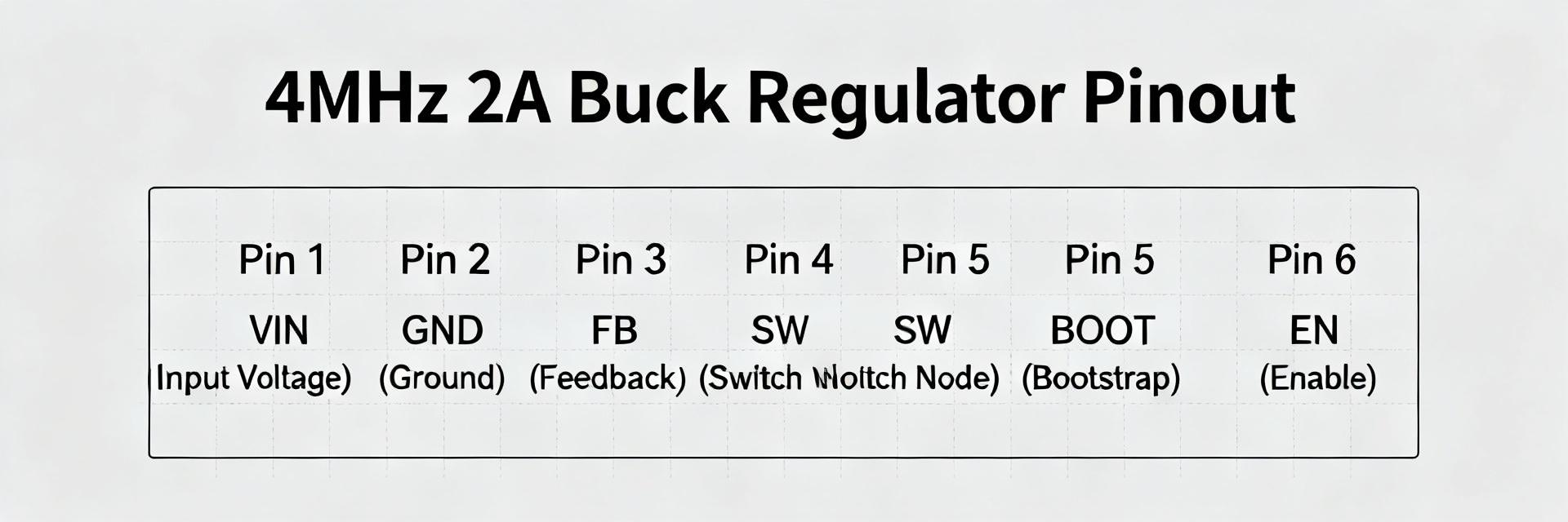
4 — Pinout, Package & Pin Functions (Method / Pinout focus)
Pin map and package options (UDFN/TMLF guidance)
Point: correct pin usage and exposed pad soldering are essential for electrical and thermal performance; Evidence: pin functions typically list VIN, SW, FB, EN, PG (power-good) and GND plus an exposed thermal pad in the package diagram; Explanation: route short traces for VIN and GND, solder the exposed pad to multiple vias to lower junction rise and ensure reliable grounding for the power stage and signal references.
Typical external components and recommended values
Point: proper external part selection ensures stability and efficiency; Evidence: recommended input cap (low-ESR ceramic, X5R/X7R), output inductor rated for >2 A with low DCR, and output caps with appropriate ESR for loop damping are specified; Explanation: select inductor with margin to avoid saturation, keep input caps close to VIN and GND pins, and follow recommended values to maintain regulator loop stability and low ripple.
5 — PCB Layout, Thermal Management & Reliability (Method / Implementation)
PCB layout best practices
Point: layout is often the single biggest determinant of measured performance; Evidence: recommended practices include tight VIN→GND decoupling loops, controlled SW node clearance, and short FB traces tied to ground returns; Explanation: implement thermal vias under exposed pad, maximize copper area for VIN and GND, and isolate SW plane to minimize radiated and conducted EMI while preserving a clean FB sense node.
Thermal calculations & derating examples
Point: estimating junction rise from converter loss lets you specify copper and cooling; Evidence: use P_loss = Pout × (1 − η) and ΘJA from package notes to estimate ΔTj; Explanation: for continuous 2 A operation allocate safety margin—improve ΘJA with vias and plane copper so junction stays below reliability thresholds at worst-case ambient.
6 — Evaluation, Troubleshooting & Implementation Checklist (Case study + Action)
Using an evaluation board and validating the datasheet claims
Point: systematic bench validation reduces integration risk; Evidence: start with no-load VIN→VOUT check, then EN sequencing, load-step tests, efficiency sweeps and thermal imaging as recommended; Explanation: document anomalies such as start-up hiccups, oscillation, or PG timing differences and iterate layout or component changes before committing to PCB revisions.
Final implementation checklist & selection tips
Point: a concise checklist accelerates production readiness; Evidence: include inductor rating, input protection, output caps, EMI filters, and test points for VIN, SW, FB, PG and temperature on the PCB; Explanation: validate EMI limit lines, ensure thermal reliefs are sufficient, and finalize BOM parts with the chosen capacitor and inductor vendors to lock performance across assemblies.
Summary
- MIC23153 delivers a 4 MHz switching solution with sub-1 V feedback and up to 2 A output, enabling compact, battery-powered point-of-load designs when component and layout guidelines are followed to control thermal and EMI impact.
- Verify DC tolerances and absolute limits against the datasheet, margin voltage references for ADCs and sequencing, and select inductors and capacitors with sufficient current rating and ESR characteristics for stable operation.
- Follow strict layout rules: short VIN/GND loops, thermal vias under the exposed pad, careful SW clearance and a clean FB return. Validate with an evaluation board, load-step testing, and thermal imaging prior to production.
FAQ
What are the recommended pinout precautions and pinout routing tips?
Keep the SW node loop area minimal, place input caps adjacent to VIN and GND pins, and solder the exposed pad to a grounded copper plane with multiple thermal vias. Route the FB trace away from noisy SW nodes, using a single-point return to the ground plane to preserve regulation accuracy and minimize EMI coupling.
How should I interpret the datasheet thermal limits for continuous 2 A operation?
Compute converter loss using measured efficiency at expected VIN and VOUT, then use package ΘJA to estimate junction rise. If junction approaches recommended maximum, increase copper area and vias or limit continuous current with derating. Plan a safety margin for higher ambient temperatures and worst-case efficiency.
What are common troubleshooting steps for MIC23153 layout-related instability?
Recheck input decoupling placement and values, verify the FB layout and return path, inspect SW node clearance and ground stitching, and confirm inductor and capacitor ratings. Use a scope to capture load-step response and switch-node ringing; add small series damping or adjust output capacitance per stability guidance if oscillation appears.
