Designers facing rising RF performance demands in wireless infrastructure must read switch specifications with operational caution: misinterpreting key metrics can erode link budget, create unwanted intermodulation, or break transmit/receive timing. This guide walks through the datasheet blocks and RF metrics engineers should prioritize, showing how to translate numbers into system-level decisions without relying on vendor marketing language.
(1) — Background: HMC349ALP4CE at a glance
Intended frequency range & target applications
Point: The datasheet lists the device’s operating band and target systems to position the part. Evidence: Typical SPDT RF switches of this family cover low‑MHz up through multiple GHz bands suitable for cellular infrastructure and test gear. Explanation: Understanding the specified band (illustrative: 100 MHz–4 GHz) clarifies whether the switch meets antenna, duplexer, or IF routing needs and whether package parasitics will affect upper‑band performance.
Key electrical and mechanical summary to extract from the datasheet
Point: Pull a concise electrical and mechanical snapshot before deeper analysis. Evidence: Scan absolute maximums, operating conditions, recommended voltages, control logic thresholds, thermal limits, and mechanical drawing. Explanation: Capturing nominal supply/current, logic levels, and thermal derating up front speeds layout decisions and prevents sourcing a part whose package pitch or thermal pad rules out intended assembly or cooling strategies.
(2) — Core RF metrics: definitions and practical significance
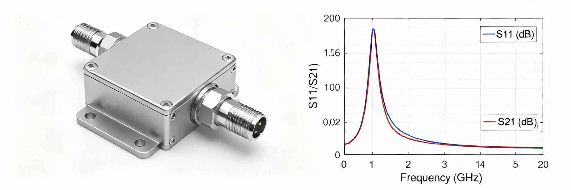
Insertion loss & return loss (VSWR)
Point: Insertion loss and return loss determine link budget and match to amplifiers. Evidence: Insertion loss is the forward power loss through the switch; return loss (or VSWR) measures mismatch. Explanation: Low insertion loss preserves margin—an illustrative 0.9–1.4 dB loss can cost several dB of system margin—and good return loss (>10–15 dB) avoids reflected power that can detune or stress preceding LNAs/PA stages.
Isolation & port-to-port leakage
Point: Isolation controls how much signal leaks between paths and affects receiver desensitization. Evidence: Isolation is frequency dependent and often degrades at band edges; package parasitics and layout can further reduce it. Explanation: Expect tens of dB of isolation in good switches; inadequate isolation near strong transmit carriers produces desensitization or spur mixing, so designers must read isolation vs. frequency and plan shielding or filter placement accordingly.
(3) — Interpreting datasheet performance numbers for HMC349ALP4CE
Typical vs. min/max values and stated test conditions
Point: Distinguish typical curves from guaranteed min/max specs and reproduce test conditions. Evidence: Datasheets present “typical” plots and guaranteed figures often measured at 50 Ω, specific bias, and defined control states. Explanation: Use guaranteed min values for margining; when a typical curve looks favorable, verify the test frequency, temperature, bias, and source impedance match your application before assuming identical performance in system tests.
Reading frequency- and temperature-dependent plots
Point: S-parameter plots and bias/temperature curves tell the real story across environments. Evidence: Insertion loss vs. frequency and isolation vs. frequency plots show trends and resonances; temperature curves show drift. Explanation: Read graph markers, interpolate intermediate points conservatively, and note any sharp roll‑offs or inflection points that could limit broadband performance or require extra margin at band edges.
(4) — Linearity, power handling and switching characteristics: what to check
P1dB, input IP3 (IIP3) and output IP3 implications
Point: Linearity specs predict intermodulation and system headroom. Evidence: P1dB reports compression; IIP3/OIP3 predict third‑order distortion. Explanation and worked example: For illustration, if IIP3 = +53 dBm (illustrative), two tones at −10 dBm each yield IM3 ≈ 2*(−10) − 53 = −73 dBc, placing IMD tones near −83 dBm absolute; designers should compare these spurious levels to receiver sensitivity and blocker budgets when selecting a switch.
Power compression, switching speed, and reliability-related metrics
Point: Check continuous and transient power limits plus switching timing. Evidence: Datasheets list P0.1dB/P1dB points, switching times, and recommended maximum input power. Explanation: Exceeding compression limits causes gain loss and distortion; switching time and cycle life affect T/R sequencing and reliability in TDD or fast‑switching test applications—designers must ensure timing margins and derate power for thermal life.
(5) — Practical selection trade-offs and a sample decision flow
Trade-off matrix: isolation vs. insertion loss vs. linearity
Point: No single metric dominates—trade-offs drive choices. Evidence: Higher isolation designs may use different topologies or larger dies that increase insertion loss or cost. Explanation: Prioritize linearity at the front end where IMD matters most; accept modest extra loss if isolation prevents cross‑talk-induced desensitization. Create a short decision flow: prioritize linearity → verify isolation across band → confirm insertion loss in worst‑case.
Minimum datasheet checklist for infrastructure designs
Point: Capture a compact checklist to compare candidates. Evidence: Essential items are insertion loss (typ/min), isolation (typ/min) across band, return loss, P1dB, IIP3, switching time, supply current, thermal limits, and package parasitics. Explanation: Recording these values consistently across parts enables apples‑to‑apples trade studies and highlights thermo‑electrical or layout constraints early.
(6) — Verification and prototyping: bench tests & layout tips
Essential bench measurements to validate datasheet claims
Point: Bench validation prevents surprises in system integration. Evidence: Key tests include VNA S‑parameter sweeps for insertion/return/isolation, two‑tone IP3 tests for linearity, and power sweeps for P1dB plus temperature/bias stress tests. Explanation: Follow matched 50 Ω setups, compensate for fixture and cable loss, and reproduce datasheet bias and control conditions when comparing results to published plots.
PCB layout and control considerations to preserve RF performance
Point: Layout decisions often determine whether datasheet performance is achievable on a board. Evidence: Rules of thumb include 50 Ω transmission lines, via stitching around ground pads, shortest RF traces to the package, and local decoupling for control pins. Explanation: Keep digital control traces away from RF paths, provide thermal vias under the exposed pad, and follow recommended land patterns to avoid added parasitics that degrade insertion loss and isolation.
Key summary
- Identify and extract operating band, package/pinout, and thermal limits from the manufacturer’s datasheet before layout decisions to avoid assembly or cooling problems.
- Prioritize guaranteed min specs (insertion loss, isolation, return loss) for margin; use typical plots for trend understanding but verify test conditions.
- Evaluate linearity and power handling (P1dB, IIP3) against system blocker and sensitivity budgets; include a short worked IM3 check during selection.
- Validate with bench tests (VNA sweep, two‑tone IP3, power sweep) and follow strict PCB layout rules—50 Ω routing, decoupling, and thermal via strategy.
Common questions
How should engineers use the datasheet insertion loss when budgeting link margin?
Use guaranteed minimum insertion loss figures when allocating link‑budget margin: subtract the worst‑case insertion loss across the operating band and include additional margin for connector/PCB and temperature effects. If only typical curves are available, reproduce test conditions or add conservative derating (e.g., +0.3–0.6 dB) to avoid underestimating loss in the field.
What is the most reliable bench method to confirm isolation claims?
Measure isolation with a calibrated VNA using a fixture that preserves 50 Ω matching and compensates for fixture loss. Sweep across the intended band and capture isolation between ports at relevant bias states; cross‑check by injecting a strong carrier and measuring desensitization at the intended receiver input to validate practical impact.
How do switching time and cycle ratings influence T/R timing in infrastructure designs?
Switching time defines minimum T/R dead‑time; cycle ratings inform expected wear under frequent switching. Ensure control logic enforces required delays to avoid transient distortion and that expected cycle count over device life does not exceed the datasheet’s reliability guidance—design for conservative margins in both timing and power to preserve uptime.
