Data-driven designers report that the FP6861E-A1S6CTR datasheet often reveals compact PCB benefit and improved inrush control compared with peer low-voltage N-channel high-side switches. You should treat this focused datasheet review as a pre-layout checkpoint: it extracts pinout clarity, the most consequential electrical specs, and practical implementation notes so you can reduce risk during PCB layout and qualification. The part number appears in key sections to help you cross-check values quickly against your system requirements.
1 — Product Overview & Key Features (background)
1.1 — What the FP6861E-A1S6CTR is and where it fits
The FP6861E-A1S6CTR is a single N‑channel MOSFET high-side power switch family member intended for USB port power switching and general power distribution on self-powered and bus-powered designs. You will find it useful where compact board area, controlled inrush, and fault reporting are required. Typical targets include downstream USB ports, power-tree branches, and embedded load switching where thermal budget and transient handling are tight.
Headline datasheet features you should call out: adjustable current limit (ILIM), low typical RDS(on) for minimal I²R loss, fault/OC reporting flag, enable/input sequencing options, and on-chip soft-start behavior. Locate the main functional blocks (switch FET, current-sense/limit, control logic, fault comparator) in the datasheet’s block diagrams and the electrical tables for device ratings and dynamic behavior; treat figures and tables as your authoritative mapping between functions and pin names when labeling nets in CAD.
1.2 — Quick specification snapshot (table suggestion)
Use a single-screen table to capture absolute max ratings, operating supply range, typical RDS(on), ILIM range, package type, and thermal theta-JA. Highlight items you must cross-check against system constraints (VDS max, continuous current, thermal derating).
| Parameter | Typical / Note |
|---|---|
| Supply (VIN) | Device operating window — confirm your USB or battery rail |
| RDS(on) | Low typical value — reduces I²R losses; check at your junction temp |
| ILIM | Adjustable range via pin — set to limit inrush and protect traces |
| Package / Theta-JA | Small package — requires PCB copper for thermal relief |
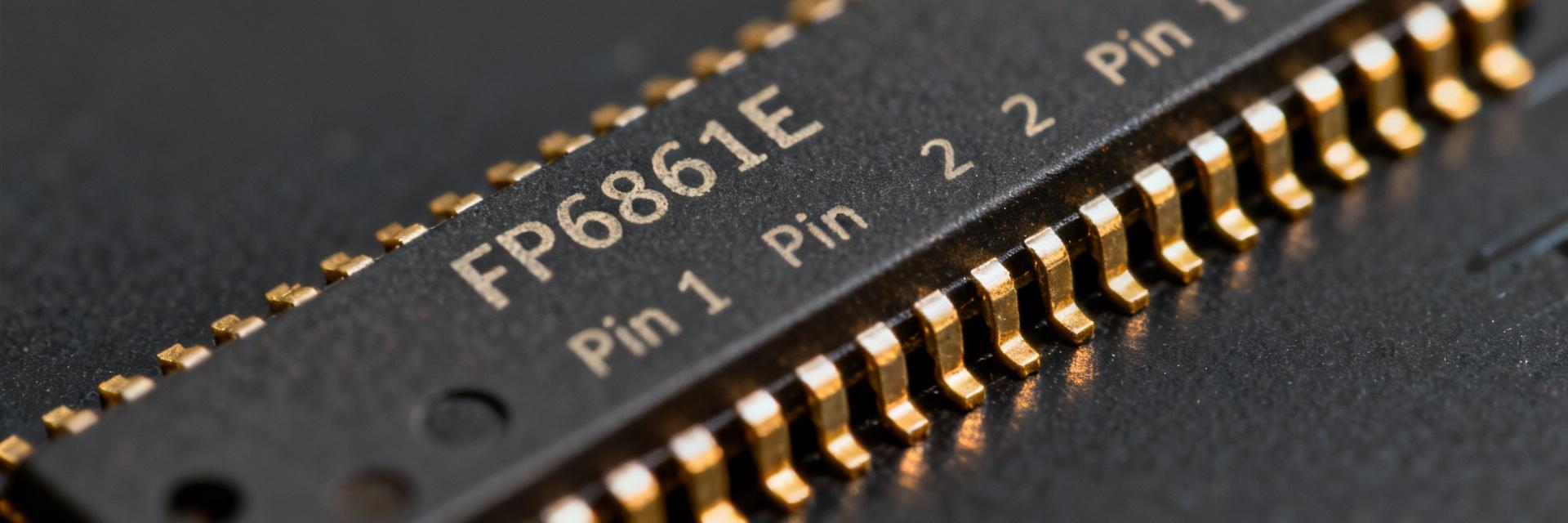
2 — Pinout Breakdown & Functional Pin Descriptions (method guide)
2.1 — Pin assignment diagram interpretation
When you read the package pinout, first identify VIN, VOUT (and note any NC / “consider as VOUT” remarks), GND, EN, FAULT/OC, and ILIM. Pin labels map to physical pads: VIN is the power-in pad, VOUT is the switched pad; keep VIN and VOUT pours separate with short, wide traces. Pinout diagrams often mark pins as NC yet recommend using them as thermal or VOUT tie points — if the datasheet states “consider as VOUT,” treat those pins as power pads and route accordingly in CAD.
Common PCB mistakes include treating NC pins as don’t-connect (then leaving useful copper off), routing high-current traces under sensitive sense/control traces, or placing decoupling far from VIN. Suggested pin-diagram caption for your CAD: “Top view — VIN pads (wide), VOUT pads (wide), GND, EN (logic), ILIM (analog adjust), FAULT (open-drain).” Label nets with clear suffixes (VIN_USB, VOUT_PORT1, EN_CPU) to avoid cross-connection errors during review.
2.2 — Pin-level electrical behavior & recommended external components
For EN: expect logic-high enable threshold; add a pull-down if you require default-off behavior (e.g., 100 kΩ). For ILIM: use the recommended resistor to set current limit — datasheet gives the resistor-to-current curve; choose resistor with 1% tolerance for repeatability. FAULT/OC is typically open-drain — pull it up to your system IO rail through 10 kΩ and add filtering (100 nF) to debounce transient events. For VOUT decoupling, place a low-ESR capacitor (e.g., 10 μF ceramic) within 5 mm of VOUT pin to stabilize soft-start and absorb surge currents.
3 — Electrical Specs Deep Dive & Performance Analysis (data analysis)
3.1 — Key static and dynamic specs to validate
Focus on RDS(on), ILIM accuracy and hysteresis, ON/OFF transition times, thermal resistance (θJA), and maximum continuous current — these electrical specs dictate thermal margins and PCB copper area. Convert RDS(on) into power loss with P = I²·RDS(on); then estimate ΔTj = P·θJA to approximate junction rise. For example, a 3 A continuous load at an RDS(on) of 0.1 Ω yields 0.9 W loss; multiply by θJA from the datasheet to get temperature rise and decide required copper.
Also validate ILIM tolerance across temperature — set the ILIM resistor so that the set-point accounts for tolerance and hysteresis; allow headroom for short-duration inrush spikes versus sustained overloads. Use the ON/OFF transition times to size snubbers or to ensure microcontroller sequencing meets EMI and inrush goals.
3.2 — Test-condition caveats & interpreting graphs
Datasheet plots are often “typical” at specified test conditions (ambient temp, pulse width). Read axis labels and legends: on-resistance vs. temperature curves show degradation at higher Tj; ILIM vs. temperature may shift several percent. Re-test transient surge and repetitive short-circuit behavior in your lab because thermal and PCB parasitics can change effective limits. Checklist: verify RDS(on) at your max expected junction, measure ILIM across temperature, and confirm thermal shutdown thresholds if present.
4 — Thermal, PCB Layout & Reliability Considerations (case / implementation)
4.1 — PCB layout best practices for high-side MOSFET switches
Route VIN and VOUT with the widest, shortest traces possible and use solid copper pours for heat spreading. Place input decoupling close to VIN pad, and place output decoupling close to VOUT. Keep sense and control traces (EN, ILIM, FAULT) physically separated from high-current routes to minimize injected noise. If pins are “NC but considered as VOUT,” tie them to the VOUT plane with short traces and thermal vias to increase conductance.
4.2 — Thermal management and derating in real-world conditions
Use θJA to estimate maximum continuous current: calculate power loss and allowable temperature rise to keep Tj below recommended reliability limits. For example, compute P_loss = I²·RDS(on); Tj = Tamb + P_loss·θJA. Increase copper area or add thermal vias if Tj approaches the device limit. During validation, capture thermal images under sustained load and implement long-run stress tests to identify hot spots early.
5 — Typical Application Circuits & Example Use Cases (case)
5.1 — Common application schematics to prototype quickly
Provide three quick circuits: 1) USB port power switch with ILIM resistor set for USB current profile and FAULT tied to MCU via open-drain; include 10 μF at VOUT. 2) Battery-fed power path where VIN is battery, EN controlled by system, and ILIM set for charge-inhibit behavior. 3) Load-switch with active fault handling: FAULT pulled to MCU with 10 kΩ and a 100 nF filter to avoid false trips. In each, place capacitors within a few millimeters of device pins and route heavy currents on the top copper layer with thermal vias beneath the package.
5.2 — Compatibility checklist for system integration
Confirm input voltage window, expected peak inrush, MCU logic levels for EN/FAULT, and thermal budget. Ask: Does ILIM cover the required inrush and sustained current? Will the package thermal path require additional copper or a heatsink? These checks prevent late-stage redesigns.
6 — Validation, Troubleshooting & Test Checklist (action)
6.1 — Pre-silicon and bench validation steps
Run VIN ramp tests to validate soft-start, step ILIM resistor values to verify current clamp, sequence enable/disable to check behavior, inject fault conditions and measure FAULT timing, and perform thermal soak tests at expected ambient and airflow. Recommended instruments: 4‑wire power supply, current pulse generator, oscilloscope with differential probes, thermal camera. Acceptable measurement tolerances: verify ILIM within datasheet tolerance and RDS(on) within typical-to-max spread under your junction temp.
6.2 — Common failure modes and fixes
Symptoms: false FAULTs — likely noise coupling on FAULT/EN; add RC filtering. Overheating under expected load — increase PCB copper or add vias beneath package. Incorrect current limit — check ILIM resistor tolerance and placement. For inrush-related trips, increase soft-start capacitance or raise ILIM set-point carefully while observing thermal impact.
Summary
- Verify the FP6861E-A1S6CTR datasheet early: confirm VIN/VOUT ratings and ILIM behavior to avoid late redesigns; cross-check RDS(on) and thermal specs against your expected current and copper area.
- Use correct pinout handling: treat NC pads marked as VOUT as power pads, place decoupling within millimeters, and separate control traces from heavy-current routes to reduce EMI and false faults.
- Validate in the lab: measure ILIM across temperature, perform VIN ramp and fault injection tests, and capture thermal images under sustained load to ensure reliability before qualification.
