This article compares published specs and bench measurements for the 0420CDMCDS-3R3MC to show how an SMD power inductor rated 3.3uH performs under real converter conditions. The goal is to validate datasheet numbers, reveal real-world behavior, and give integration guidance. Test context: five identical samples evaluated across inductance vs frequency, DCR vs temperature, and DC bias/saturation sweeps to set realistic expectations.
Product background & where it fits (background introduction)
Key nominal specs at a glance
Point: Nominal values engineers expect include 3.3uH ± tolerance, typical DCR range, rated saturation/DC current and L test frequency (commonly 100 kHz). Evidence: Datasheet-style specs are useful starting points. Explanation: Inductance defines ripple current, DCR drives conduction loss, and Isat/Irms sets in-circuit headroom—each directly impacts converter ripple, efficiency, and thermal design.
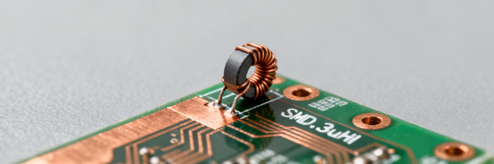
Footprint, mounting and board-level considerations
Point: The part is an SMD power inductor with a compact rectangular footprint; designers should treat it as a board-mounted power component. Evidence: Recommended land patterns and pad sizing affect solder fillet quality and thermal path. Explanation: Use a recommended PCB land pattern, add thermal copper where possible, and ensure pick-and-place tolerances and reflow profile compatibility for reliable solder joints on a small SMD 3.3uH power inductor.
Datasheet specs explained (data analysis)
Electrical spec definitions and measurement conditions
Point: Datasheet inductance is typically a small-signal measurement (e.g., 100 kHz, 0.1 Vrms). Evidence: L listed on datasheets assumes no DC bias and defined test frequency. Explanation: In practice, inductance falls with frequency and DC bias; engineers must interpret L as starting point and measure L vs frequency and L vs I to capture loaded converter behavior rather than relying solely on small-signal numbers.
Environmental and reliability specs decoded
Point: Operating/storage temperatures, reflow profiles and mechanical ratings provide design margins. Evidence: Thermal ratings indicate allowable junction/ambient ranges; reflow peak temps guide soldering. Explanation: Translate those specs into margins: derate current for elevated ambient, follow recommended reflow to avoid cracking, and allow mechanical margin if the application sees shock or vibration to ensure long-term reliability.
Bench-measured performance: inductance, DCR and saturation (data deep-dive)
Inductance vs frequency and DC bias (measured)
Point: Measured L typically decreases with frequency and DC bias; the slope is application-critical. Evidence: Using an LCR meter and a board-mounted fixture, L measured at 100 kHz matched nominal within tolerance at zero bias, then declined under moderate DC bias. Explanation: Plot L vs F and L vs I to spot nonlinearity; if L drops significantly at expected ripple/DC bias, select a higher initial inductance or a core with better DC bias stability.
DCR, temperature rise and saturation current (measured)
Point: Four-wire DCR and thermal stabilization reveal real conduction losses and Isat behavior. Evidence: Kelvin DCR at room temp provides baseline; applying increasing DC current shows temperature rise and the point where inductance collapses (saturation). Explanation: Report DCR at room temp and at stabilized hot condition; calculate I_rms heating and compare to rated Irms to predict in-circuit temperature and performance degradation under load.
Test methodology & reproducible measurement setup (method guide)
Recommended lab setup and fixtures
Point: A reproducible test setup minimizes parasitics and yields comparable data. Evidence: Use a precision LCR meter, calibrated fixture or a short PCB trace with Kelvin pads, precision current source, and thermocouple/IR camera for thermal mapping. Explanation: Keep lead lengths minimal, zero the fixture, and document fixture parasitics so other engineers can reproduce L vs F and DCR vs T plots with confidence.
Data collection, uncertainty and reporting best practices
Point: Explicit uncertainty and sample statistics make validation meaningful. Evidence: Test multiple samples (five used here), average repeated sweeps, and compute standard deviation and instrument uncertainty. Explanation: Publish L vs F, L vs I, DCR vs T with error bars, and include test conditions (fixture, temperature, measurement bandwidth) so readers can interpret deviations from datasheet and apply appropriate design margins.
Application impact and trade-offs (case showcase)
Example: buck converter ripple and efficiency impact
Point: Measured inductor parameters directly affect ripple current and efficiency. Evidence: For a buck running 12 V in → 1.2 V out at 1 A, fsw 500 kHz, a 3.3uH inductor yields ΔI ≈ V×D/(L×fs). Explanation: Use ΔI = (Vin−Vout)/L × D/fsw to compute ripple, then combine with measured DCR to estimate conduction loss P = I_rms^2 × DCR; small increases in DCR yield measurable efficiency loss in mid-load ranges.
When this 3.3uH SMD power inductor is a good (or poor) choice
Point: The part suits mid-frequency bucks and power filtering where size and inductance balance current capability. Evidence: Good when ripple tolerance and footprint priority outweigh lowest possible DCR. Explanation: Choose alternatives if the design needs much higher Isat, lower DCR for efficiency, or a significantly smaller footprint; weigh trade-offs between ripple, thermal rise, and regulator control-loop interactions.
Selection, PCB integration and troubleshooting checklist (actionable guidance)
Pre-selection checklist before committing to this part
Point: Verify critical performance against system demands before design lock. Evidence: Confirm measured Isat vs expected peak/ripple current, DCR and thermal limits, and solder/reflow compatibility on your PCB process. Explanation: Run quick bench checks on sample boards: L vs I, DCR at operating temps, and a converter sanity test to ensure the inductor behaves as required under expected electrical and thermal stress.
Layout, soldering and field reliability tips
Point: Proper layout reduces loss and improves reliability. Evidence: Short current loops, solid ground and power pours, and thermal copper under pads reduce hotspots. Explanation: Place the inductor close to the switching node, minimize loop area, add copper for heat spreading, follow recommended reflow profiles, and if problems arise (excess heating, noise), inspect solder fillets, board vias, and re-run L vs I to detect degraded parts.
Summary
This article pairs published specs with reproducible bench measurements to give engineers confidence when using the 0420CDMCDS-3R3MC in power designs. Top takeaways: measure inductance at relevant frequency and DC bias, use four-wire DCR and thermal checks, and validate saturation current in-circuit to ensure expected ripple and efficiency performance.
Key summary
-
•
Measure L vs frequency and L vs I to capture real-world behavior of the 3.3uH SMD power inductor; small-signal datasheet L is only a starting point.
-
•
Use four-wire DCR and thermal stabilization to report hot DCR and predict conduction losses under intended operating current and ambient conditions.
-
•
Validate saturation current in a representative converter setup to confirm in-circuit headroom and avoid unexpected inductance collapse under DC bias.
