The LPC802M001JDH20J is a purpose-built, ultra-compact 32-bit Cortex-M0+ MCU family member optimized for low‑power embedded designs; it advertises a maximum CPU clock of around 15 MHz, an entry‑level flash footprint, multi‑channel ADC and common serial interfaces. This introduction frames what the part actually delivers for US product and prototype workflows and points engineers toward the official datasheet for final verification.
Practical use favors tiny battery‑powered nodes, low‑cost consumer controls and compact sensor endpoints where package size and power dominate decisions. Read the official datasheet revision and errata before design lock: focus first on electrical characteristics, memory map and pinout to verify the exact specs for your chosen variant.
Why the LPC802M001JDH20J matters (background)
Target applications and product fit
Point: The MCU is aimed at minimal‑function, cost‑sensitive embedded products. Evidence: Typical fits include simple sensors, basic control nodes and battery‑powered IoT endpoints where MCU functions are modest. Explanation: Designers trade off raw compute and feature set for low BOM cost, small PCB area and low quiescent current—making this part a sensible choice for multi‑year battery targets and compact consumer devices.
Official datasheet & revision notes
Point: Always consult the official datasheet PDF and current errata. Evidence: The datasheet contains the electrical tables, memory map and pin descriptions that determine board‑level decisions. Explanation: Obtain the datasheet from the manufacturer’s website or authorized documentation portal, check the document revision and errata IDs, and read electrical characteristics, memory mapping and pinout pages first to catch package variants and absolute maximums before PCB layout.
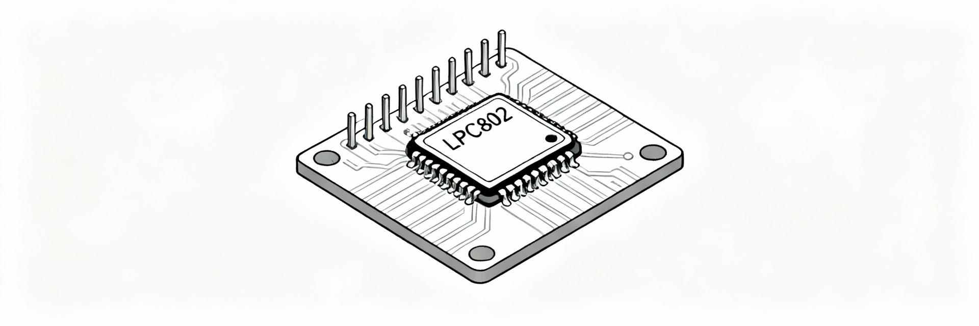
LPC802M001JDH20J: Key electrical and memory specs (data deep‑dive)
Core, clock and voltage specs
Point: Cortex‑M0+ core with modest maximum clock and a single‑supply domain suits low‑power designs. Evidence: The part targets a maximum CPU clock around 15 MHz with standard internal oscillator options and a single‑supply operating window typical for low‑voltage MCUs. Explanation: Clock and supply choices directly affect performance and current draw—lower clock and reduced core voltage yield proportional savings in active current, so configure clocks only as high as needed for the workload to maximize battery life.
Memory and storage layout
Point: Memory is sized for compact applications. Evidence: This family is an entry‑level flash class (typical devices in this family sit in the ~16 KB flash region) with a small SRAM block sufficient for lightweight stacks and buffers; boot ROM features often provide a minimal bootloader. Explanation: Flash and RAM limits constrain large frameworks and over‑the‑air images; keep firmware lean, use link‑time garbage elimination, and verify the exact flash/RAM numbers in the datasheet before committing to production.
LPC802M001JDH20J peripherals & interfaces breakdown (data deep‑dive)
Analog peripherals: ADC & comparators
Point: On‑chip analog supports basic sensing. Evidence: Expect a multi‑channel ADC in the 10–12 bit class with selectable reference options and a handful of channels suitable for temperature, light and battery sensing. Explanation: ADC sampling strategy matters—use averaging, proper reference selection and input conditioning to meet measurement accuracy without inflating firmware complexity or power use.
Digital interfaces: I2C, SPI, USART, timers, GPIO
Point: The MCU exposes the essential serial and timer peripherals for common embedded tasks. Evidence: Typical offerings include I2C, SPI, and at least one USART, basic timers with PWM capability, and GPIOs with pin‑mux constraints; DMA is generally absent or limited on entry‑class devices. Explanation: Multiplexing pins requires planning—map sensors and debug pins to avoid conflicts, and budget throughput expectations around single‑master SPI/I2C bursts rather than high‑bandwidth streaming.
Performance, power consumption and thermal limits (data analysis)
Power modes, current draw and battery planning
Point: Power profiles determine battery life more than peak CPU speed. Evidence: Typical devices show low‑microamp deep‑sleep and modest active currents at low MHz; a simple battery‑life calculation uses average current = duty%*active_current + (1-duty%)*sleep_current. Explanation: Example: with 1% active duty, 5 mA active peaks and 5 µA sleep, average current ≈55 µA; a 2,000 mAh cell yields ~36,000 hours (~4 years) of theoretical life—use datasheet figures for accurate planning and include radio or sensor currents if present.
5 mA
0.005 mA
0.055 mA
Thermal, package and operating conditions
Point: Small packages limit thermal dissipation and continuous high‑current operation. Evidence: The part is available in compact 20‑pin small‑outline packages with standard commercial temperature ranges; continuous high‑power draw forces derating. Explanation: For sustained loads, follow the datasheet thermal guidance, avoid heating from nearby regulators or radios, and design for the worst‑case ambient to keep junction temperature within limits for reliable lifetime.
Hardware integration & PCB guidelines (method guide)
Pinout, package options and footprint tips
Point: Correct footprint and pin assignments prevent rework. Evidence: Critical pins include VDD, VSS, RESET and debug lines (SWDIO/SWCLK) in the 20‑pin pinout; small packages constrain routing and decoupling placement. Explanation: Place a primary 0.1 µF decoupling capacitor adjacent to VDD pins, keep RESET and debug traces short, and reserve a ground pour under the MCU to stabilize return paths and reduce EMI.
Power supply, clock and reset circuit recommendations
Point: Simple power and reset circuits improve reliability. Evidence: Use a 0.1 µF ceramic decoupling plus a 1 µF bulk cap on VDD, a pull‑up on RESET (10 kΩ) and Schmitt‑trigger input for external reset if used. Explanation: If an external oscillator is required, follow layout guidance for crystal or oscillator modules; otherwise use internal RC with calibration to reduce component count and board area.
Firmware, programming and development workflow (method guide)
Bootloader, debug and programming interfaces
Point: Multiple programming paths simplify prototyping. Evidence: Devices typically provide a ROM boot path and SWD debug interface; flashing is possible with a standard SWD‑compatible tool using SWDIO/SWCLK plus VDD/GND and optional RESET. Explanation: During prototyping, keep SWD accessible and plan for a production debug header or programming pogo pad; verify minimal signals needed from the datasheet before wiring fixtures.
Minimal BSP & example start‑up sequence
Point: A compact startup saves flash and RAM. Evidence: Minimal init includes oscillator setup, GPIO defaults, ADC calibration and low‑power configuration. Explanation: Initialize clocks to the lowest frequency that meets timing, set unused pins to defined low‑power states, sample ADC only when needed, and use link‑time optimization and stripped C libraries to minimize footprint.
Application examples & design checklist (case + action suggestions)
3 concise example projects
Example 1: Battery environmental sensor — peripherals: ADC, I2C temp/humidity, low‑power timer; expected memory: small bootloader + compact sensor stack (~8–16 KB flash); power: periodic wake, sample, transmit, deep‑sleep strategy. Example 2: Simple motor/tactile control — peripherals: PWM timer, GPIO, small state machine; memory: modest firmware for input debounce and control. Example 3: UART/I2C bridge — peripherals: USART and I2C, minimal buffering; memory and CPU suffice for low‑throughput bridging.
Design & purchasing checklist
Point: Confirm variant details before ordering. Evidence: First checklist item: obtain the official datasheet and verify the exact part marking, revision, and the detailed specs for the package variant you plan to buy. Explanation: Also confirm package type, programming/debug adapter compatibility, order samples for layout verification, and ensure supply continuity for production quantities.
Summary
-
The LPC802M001JDH20J is a compact, cost‑focused Cortex‑M0+ option for tiny, low‑power embedded designs; verify flash/RAM and electrical numbers in the official datasheet before committing.
-
Plan power early: use low duty cycles, minimal clocks, and accurate battery‑life calculations based on datasheet current figures.
-
Prototype with SWD debug access, correct decoupling and pin‑mux planning to catch layout issues before production.
