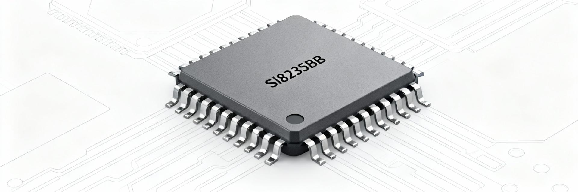
Point: The SI8235BB is a dual-channel isolated gate driver rated for approximately 4 A peak drive and ~2.5 kVrms isolation, figures that immediately frame its suitability for medium- to high-voltage power stages. Evidence: Those peak-current and isolation numbers define how quickly a driver can charge/discharge gate capacitance and what isolation envelope it supports. Explanation: This article translates those datasheet values into measurable on-board performance, layout actions, and thermal realities so designers can predict behavior in real converters and motor inverters.
Background: Why isolated gate drivers matter in modern power systems
Isolation, safety and regulatory context
Point: Galvanic isolation protects low-voltage control from high-voltage power and supports regulatory creepage/clearance requirements. Evidence: an isolation rating near 2.5 kVrms indicates robust dielectric withstand capability and helps set working-voltage class and PCB creepage spacing. Explanation: Designers map isolation ratings to system insulation by selecting creepage/clearance per the target working voltage and pollution degree, placing barrier tracks and slotting appropriately so the isolated gate driver meets system safety and surge expectations.
Typical topologies and functional roles
Point: Isolated gate drivers are used for half-bridges, full bridges and high-side gate drive where bootstrapping is inadequate or multi-level isolation is preferred. Evidence: dual-channel isolation consolidates two gate drives into one package, simplifying board routing and ensuring matched timing between channels. Explanation: In converters driving Si, SiC or GaN switches, a dual isolated driver reduces component count and eases layout in multiphase or bridged topologies while providing independent isolated supplies and balanced propagation behavior.
SI8235BB performance specifications overview
Key electrical specs to benchmark
Point: Engineers should benchmark peak output current (4 A peak), propagation delay, input-to-output isolation voltage, common-mode transient immunity (CMTI), UVLO thresholds, gate voltage swing and output fault behavior. Evidence: peak drive current governs how fast gate charge is delivered; propagation delay and skew determine timing margins; CMTI quantifies immunity to high dv/dt events. Explanation: Tracking these metrics during validation links switching losses, timing margins and transient immunity to observed device stress—enabling safe switching-environment specification and coordinated gate resistor selection.
Thermal, SOA and reliability considerations
Point: Peak current ratings do not equal continuous capability; thermal derating and package thermal resistance define safe continuous operation. Evidence: driver pulses at high repetition rates create average power that must be removed through PCB copper, vias and convection; SOA limits may be reached well before peak specs are stressed. Explanation: Convert peak-current capability into practical continuous drive by calculating energy per switching event, average power for given switching frequency and duty cycle, then use PCB thermal paths and derating curves to set maximum sustainable gate drive activity.
Quick visual metrics
Notes: bar widths are relative visual indicators for quick comparison; validate against full datasheet graphs for precise thermal/SOA limits.
SI8235BB lab testing & real-world performance
Recommended test setup and measurement procedures
Point: Accurate measurement requires careful probing, controlled decoupling and safe isolation practices. Evidence: use short ground leads or isolated probes for return, place high-frequency decoupling capacitors within millimeters of supply pins, and maintain isolation during high-voltage testing with proper fixture clearances. Explanation: A recommended procedure: mount DUT on a representative PCB, stitch ground with vias, place scope probe ground as a spring or use an active probe, measure rise/fall times, propagation delay and peak current under representative gate-charge loads while monitoring driver temperature and isolation integrity.
Interpreting results and common failure modes
Point: Deviations from datasheet values point at layout or supply problems; common failures include false switching, thermal foldback and latch-up. Evidence: slower-than-expected edges often stem from excessive loop inductance or undersized decoupling; CMTI failures correlate with large common-mode dv/dt and insufficient shielding. Explanation: When observed rise/fall times are long, inspect gate loop area and decoupling; if spurious switching appears during high dv/dt, add local common-mode filtering, increase gate resistance or improve isolation routing and retest for reliability.
Comparative scenarios & application case studies
High-frequency wide-bandgap converter scenario
Point: Driving SiC/GaN at high dv/dt amplifies demands on timing, CMTI and gate-charge delivery. Evidence: faster edges lower switching loss but raise EMI and stress the driver and transistor; repeated fast pulses increase average driver dissipation. Explanation: Quantify trade-offs by measuring switching loss vs. EMI at multiple gate resistor values, ensure CMTI margins exceed expected dv/dt, and size thermal path and decoupling so the gate driver maintains specified rise/fall times without thermal throttling at the target switching frequency.
Motor drive / inverter scenario
Point: Continuous operation in motor inverters emphasizes thermal management and deadtime control. Evidence: bootstrapped supplies may be convenient for low-side drivers, but multiphase systems benefit from isolated supplies to avoid bootstrap recharge complications. Explanation: A dual isolated gate driver simplifies multi-phase layouts by providing matched channels; designers should tune deadtime to prevent cross-conduction, monitor continuous junction temperatures, and verify long-term reliability under expected ambient and load conditions.
Design checklist & optimization tips for best performance
PCB layout, decoupling and EMI mitigation
Point: Prioritized layout and decoupling yield the best measured rise/fall times and minimize overshoot. Evidence: place decoupling caps adjacent to driver VCC pins, use Kelvin routing for gate returns, and minimize gate-to-source loop area to reduce inductive overshoot. Explanation: stepwise checklist—1) short, wide power loops with solid copper pours; 2) local high-frequency decoupling and bulk reservoir; 3) dedicated return vias and Kelvin gate traces; 4) place gate resistors close to driver outputs; 5) add snubbers or RC damping to control ringing.
Thermal management and derating guidelines
Point: Balance gate resistor choice and copper heatsinking to manage switching losses and limit driver temperature rise. Evidence: lower gate resistance speeds edges but raises peak di/dt and EMI; larger copper areas and thermal vias reduce driver junction temperature. Explanation: Rule-of-thumb: for Si MOSFETs at moderate frequency, start with 5–20 Ω; for SiC/GaN at high frequency, consider 1–10 Ω with stronger thermal mitigation; always validate by measuring driver case temperature and adjusting resistor and copper accordingly.
Summary
-
The dual-channel isolated gate driver delivers strong transient drive and robust isolation; real-world performance hinges on layout, decoupling, and thermal strategy and must be validated under representative gate-charge and dv/dt conditions.
-
Benchmark key specs—peak current, propagation delay, CMTI and isolation voltage—using a controlled test fixture; interpret deviations as layout, decoupling or supply issues and iterate accordingly.
-
Prioritize thermal paths, gate resistance tuning and EMI controls early in design: follow the measurement procedures, apply the layout checklist, and perform thermal and CMTI verification prior to system integration.
