Engineers continue to specify the ACPL-W340-560E for isolated gate-drive tasks because it pairs reinforced isolation with a 1.0 A peak output capability and a datasheet-specified isolation withstand rating of 5600 Vrms, delivering predictable isolation and drive for medium-power inverters. This article uses those headline figures to guide practical datasheet interpretation, gate-driver timing and current budgeting, PCB/thermal layout practices, and a compact bench-test checklist to validate real-world behavior.
— Quick background & key specs (background introduction)
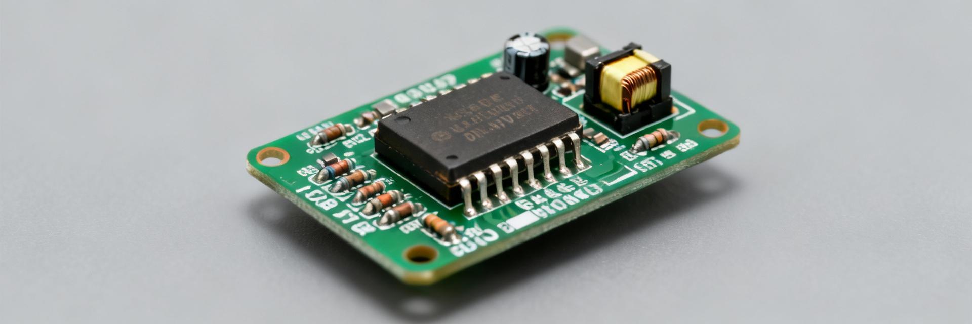
— What the ACPL-W340-560E is
Point: The device is an isolated optocoupler designed for direct gate-drive use; Evidence: manufacturer datasheet lists reinforced isolation at ~5600 Vrms and peak output current around 1.0 A; Explanation: that combination makes the part suitable where galvanic separation and short-duration drive pulses are required while keeping the drive circuitry compact and board-mountable.
— When to pick this part vs. a standard driver
Point: Choose this part when isolation and modest peak drive matter more than sub-nanosecond timing; Evidence: propagation and rise/fall timing in the datasheet imply practical PWM operation up to mid-hundreds of kHz with proper resistor choices; Explanation: if your design needs reinforced isolation, short gate-charge bursts (hundreds of mA–1 A) and a compact footprint, this part fits; for multi-amp continuous drive or very high-frequency switching, consider dedicated isolated gate-driver ICs and validate using the datasheet curves.
— Datasheet deep-dive: static & DC electrical characteristics (data analysis)
— Input LED and input-side parameters
Point: Translate input LED specs into a resistor for MCU/logic drive; Evidence: typical LED forward voltage is ~1.2 V and recommended LED drive ranges often center at 5–20 mA per the datasheet; Explanation: for a 3.3 V MCU pin and target IF = 10 mA, R = (3.3 V − 1.2 V) / 10 mA ≈ 210 Ω. Always check the datasheet's input CTR/transfer or recommended LED current and derating for sustained operation at elevated ambient temperature.
— Output stage: current capability, voltage swing, and DC limits
Point: Map DC output specs to gate-charge needs; Evidence: output is specified for peak pulses near 1 A with guaranteed logic-level voltages close to the supply rails; Explanation: for a MOSFET with effective gate capacitance Cg = 1,000 pF switching across ΔV = 15 V, gate charge Q ≈ Cg·ΔV = 15 nC. To move that charge in 100 ns requires I = Q/t = 15 nC / 100 ns = 0.15 A peak, well under the 1 A peak capability for short pulses; use the datasheet absolute maximums to size continuous vs pulsed workloads.
— Gate driver dynamic performance & switching specs (data analysis / gate driver)
— Timing: propagation delay, rise/fall time, and jitter
Point: Timing figures determine dead-time and synchronization strategy; Evidence: typical propagation delay figures on the datasheet are at microsecond or sub-microsecond scale and rise/fall times are given in the tens to hundreds of nanoseconds range; Explanation: budget one propagation delay plus two rise/fall windows per transition when setting FPGA/MCU dead-time. Example: if tpd ≈ 1 μs and tr ≈ 50 ns, set dead-time ≥ 1.1 μs plus margin; verify with bench captures of input-to-output delay under real load to capture jitter and worst-case delay.
— Dynamic current capability and switching waveform behavior
Point: Short high-current pulses during dV/dt events are allowed but thermally limited; Evidence: datasheet dynamic curves show permissive peak currents at low duty cycles and derating with pulse width/temperature; Explanation: use the output current vs time graph to compute safe pulse widths—e.g., at 1 A peak the device may permit only microsecond-scale pulses at high repetition rates; derive allowable duty cycle from the thermal energy per pulse and the thermal time constant provided in the datasheet.
— Application design & PCB implementation (method / how-to)
— Recommended gate-drive circuit topologies & component choices
Point: Use a single-ended gate-drive schematic with series gate resistor and proper decoupling; Evidence: datasheet absolute maximums define supply pins and gate-source tolerance; Explanation: pick gate-resistor Rg to trade speed vs overshoot: with drive rail VDD = 15 V and desired peak Ipk ≤ 1 A, Rg ≥ VDD / Ipk = 15 Ω. If you accept faster edges and higher Ipk, reduce Rg but verify ringing and VGS overshoot with the scope. Include a clamp/snubber and a bleeder resistor when driving large gate charge or long cable runs.
— PCB layout, isolation, and thermal/creepage best practices
Point: Layout choices preserve isolation and minimize parasitics; Evidence: datasheet-recommended creepage for the specified Vrms and general isolation practice call for several millimeters of clearance and segregated return planes; Explanation: keep input and output grounds separated, place bypass caps within 2–3 mm of supply pins, route high-current loops short and wide, and target creepage distances of 8–12 mm for the listed isolation level. Validate thermal behavior by measuring package temperature rise under worst-case switching to ensure junction limits are not exceeded.
— Use cases, testing & verification (case study + bench)
— Typical application examples & where this device excels
Point: The device excels in medium-voltage isolated gate drive and isolated PWM outputs; Evidence: reinforced isolation and short-pulse drive capability match inverter-leg and industrial converter needs; Explanation: examples include half-bridge gate isolation in motor drives where isolation voltage and brief 1 A drive pulses are required, and isolated PWM for industrial I/O. For each, key datasheet parameters are isolation rating, peak output current, propagation delay, and thermal limits.
— Bench tests to validate datasheet claims
Point: Run a short checklist of measurements to confirm real-world behaviour; Evidence: datasheet gives test conditions to reproduce—input current, supply rails, and load conditions; Explanation: suggested tests: (1) measure propagation delay with a pulse generator and scope (100 MHz+ bandwidth, 10× probes), (2) capture rise/fall under a calibrated gate load (e.g., 1 nF), (3) deliver controlled current pulses to verify peak capability and thermal response, and (4) perform isolation withstand tests per the datasheet conditions using certified equipment. Acceptable variance: typical figures ±20% vs datasheet typical, always below datasheet maximums.
— Troubleshooting & practical checklist for production (action)
— Common failure modes and fixes
Point: Failures are usually layout- or stress-related; Evidence: typical issues seen in production are ringing from low Rg, supply instability from missing decoupling, and thermal overstress from repeated high-energy pulses; Explanation: fixes—raise Rg in 5–20 Ω steps to tame ringing, add or relocate 0.1 μF decoupling within 2–3 mm of device power pins, reduce pulse duty cycle or add heat-sinking. For a failed unit, check gate resistor value, decoupling placement, and measure package temperature under load.
— Pre-production and compliance checklist
Point: A concise verification list prevents costly recalls; Evidence: datasheet absolute maximums and test conditions drive the checklist; Explanation: before volume: confirm input resistor sizing and LED current, verify propagation delay and rise/fall under target load, perform isolation withstand per datasheet, ensure layout creepage/clearance targets, and validate thermal performance under worst-case switching. Keep test records aligned with the manufacturer datasheet test conditions for compliance.
— Key summary
-
The device combines reinforced isolation and short-pulse 1 A output capability, making it suitable for isolated gate-drive roles in medium-power converters; sizing gate resistors and timing per datasheet ensures robust operation.
-
Translate LED Vf and desired IF into a resistor: example 3.3 V MCU, IF=10 mA → ~210 Ω; always verify with the datasheet input curve.
-
For a 1,000 pF gate at 15 V, Q ≈ 15 nC; to switch in 100 ns needs ~0.15 A peak, under the device's short-pulse capability—use datasheet dynamic curves to set pulse widths.
— Common questions and answers
How do I verify propagation delay and timing on the device?
What gate resistor value should I start with in prototypes?
How should I test isolation before production?
Conclusion / Summary
Reading the ACPL-W340-560E datasheet with a focus on input LED constraints, output peak-current windows, timing budgets, and thermal derating allows engineers to size resistors, set FPGA/MCU dead-time reliably, and lay out PCBs for safe operation. Practical next step: on your first prototype, run the input-to-output propagation delay test under the targeted gate load and temperature to validate timing margins before scaling to production.
