Point: In current power-conversion and motor-drive designs, isolated gate-drive performance can determine switching losses and system reliability. Evidence: Benchmarks show gate-drive optocouplers with >30 kV/µs CMTI and sub-1 µs propagation delay reduce false triggering in high dv/dt environments. Explanation: This article distills the ACPL-W340-500E datasheet into the critical numbers designers need; the term datasheet appears here to flag source context.
Point: The goal is practical evaluation and integration guidance. Evidence: Readers expect concise extraction of input/output electricals, isolation/CMTI, timing and thermal limits. Explanation: With targeted takeaways and tables, designers can map datasheet numbers to gate-charge budgets and layout constraints before lab validation.
Background: What the ACPL-W340-500E Is and Where It Fits
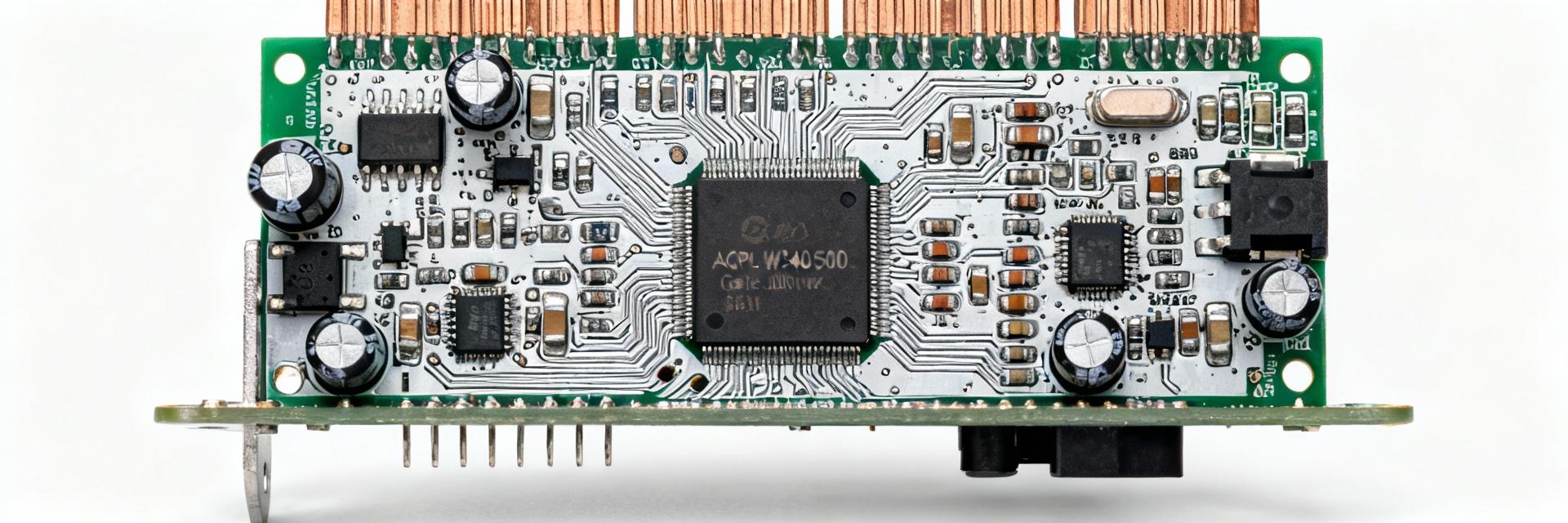
Device overview and package
Point: The ACPL-W340-500E is an isolated gate-drive optocoupler with an integrated power output stage suitable for driving IGBT and power MOSFET gates. Evidence: The datasheet groups mechanical drawing, pinout and absolute maximum ratings in the initial sections for quick reference. Explanation: Designers should consult those sections for footprint, pin count and max stress limits before schematic capture and PCB land pattern creation.
Target applications and design goals
Point: Typical application spaces include motor drives, inverter stages and high-power supplies that demand fast, robust isolation. Evidence: The device targets drive current, isolation and switching-speed performance metrics critical to these topologies. Explanation: Long-tail queries such as "ACPL-W340-500E gate drive optocoupler specs" or "optocoupler for IGBT gate drive" reflect the practical selection criteria engineers use.
Key Electrical Specifications (datasheet deep-dive)
Input (LED) electrical parameters to highlight
Point: Input LED specs determine required drive circuitry and input resistor when interfacing logic. Evidence: The datasheet lists DC forward current (If), forward voltage (Vf typ/max), input threshold and input power per channel under specified test conditions. Explanation: Use those values to size series resistors, to ensure the LED sees the correct current at your input logic voltage and to avoid overstress during fault conditions.
Output and supply-stage parameters to highlight
Point: Output capability governs achievable dV/dt control of gate charge and switching energy. Evidence: Extract output DC/peak current, output voltage range, saturation/drop, recommended VCC and typical load conditions from the datasheet tables. Explanation: Comparing typical vs. maximum values shows how much current is available for fast gate charging and how that translates to rise/fall times for a given gate charge.
| Parameter | Test Condition | Typical / Max |
|---|---|---|
| DC forward current (If) | DC, specified Ta | See datasheet If rating |
| Forward voltage (Vf) | If = specified mA | Vf typ / max |
| Input threshold | Specified test circuit | Threshold current / voltage |
Isolation, CMTI and Reliability Data (performance-critical metrics)
Isolation ratings, creepage/clearance and test conditions
Point: Isolation specs protect low-voltage control from high-voltage power stages. Evidence: The datasheet provides rated isolation voltage, isolation-test method, and any working/reinforced insulation notes plus recommended PCB creepage/clearance. Explanation: Designers must map those numbers to system-level requirements and enforce minimum PCB spacing, conformal coating decisions and standoff clearances.
Common-mode transient immunity (CMTI) and lifetime/reliability data
Point: CMTI defines immunity to fast common-mode transients that otherwise cause false triggering. Evidence: The datasheet reports CMTI (kV/µs) with explicit test conditions; MTBF and operating temperature ranges are listed for reliability planning. Explanation: Use datasheet CMTI and ambient/operating temperature specs to create derating rules and to predict behavior in high dv/dt topologies.
Timing, Switching and Thermal Performance (performance)
Timing and dynamic behavior
Point: Propagation delay and rise/fall times shape dead-time and shoot-through protection requirements. Evidence: The datasheet specifies propagation delay, rise/fall times and the test load circuits used to measure timing. Explanation: Designers should reference those test conditions when modeling dead-time margins and when sizing gate resistors to meet both switching-speed and EMI goals.
Thermal considerations and limits
Point: Thermal resistance and max junction temperature determine continuous operating capability under load. Evidence: The datasheet lists junction-to-ambient and junction-to-case thermal resistances plus maximum junction temperature and derating curves. Explanation: Implement PCB copper, decoupling and part placement strategies to keep junction temperature within safe limits when driving large gate charges repeatedly.
| Spec | Condition | Note |
|---|---|---|
| Peak output current | Pulse test | Impacts gate charge slew |
| CMTI | Specified dv/dt test | High dv/dt immunity reduces false triggers |
| Propagation delay | Measured with load | Used in dead-time calc |
Design & Integration Guide (practical how-to)
Typical gate-drive circuits and component recommendations
Point: Reference circuits translate datasheet numbers into component roles. Evidence: Typical circuits use a series gate resistor, a pull-down, clamp (TVS/snubber) and sometimes a bootstrap supply for high-side drives. Explanation: Use output current and timing specs to pick gate resistors and to decide whether active Miller clamps or stronger pull-downs are required for a given MOSFET or IGBT gate charge.
PCB layout, grounding and EMI mitigation tips
Point: Layout is critical for isolation, noise control and thermal performance. Evidence: The datasheet calls out creepage/clearance and recommends decoupling near VCC pins; practical rules include separating noisy returns and minimizing loop inductance. Explanation: Place decoupling close to the device, route return paths cleanly, provide test points and use dedicated isolation slots or conformal coating where required.
Troubleshooting, Comparison and Application Examples (actionable)
Common failure modes and debug checklist
Point: Common issues include no output, weak drive, false triggering or thermal shutdown. Evidence: The datasheet’s absolute maximums and timing/CMTI specs provide pass/fail thresholds for measurements. Explanation: Check input drive current, VCC rails, board clearances and confirm CMTI margins with a controlled dv/dt test to isolate the root cause quickly.
Example application scenarios and selection checklist
Point: Sizing for a MOSFET requires mapping gate charge and switching frequency to drive energy and thermal budget. Evidence: Use datasheet peak output current and timing to calculate charge time and average power dissipation during switching. Explanation: Final procurement should confirm isolation rating, CMTI, peak output current and timing against lab tests: turn-on/off waveforms, temperature rise and isolation withstand tests.
