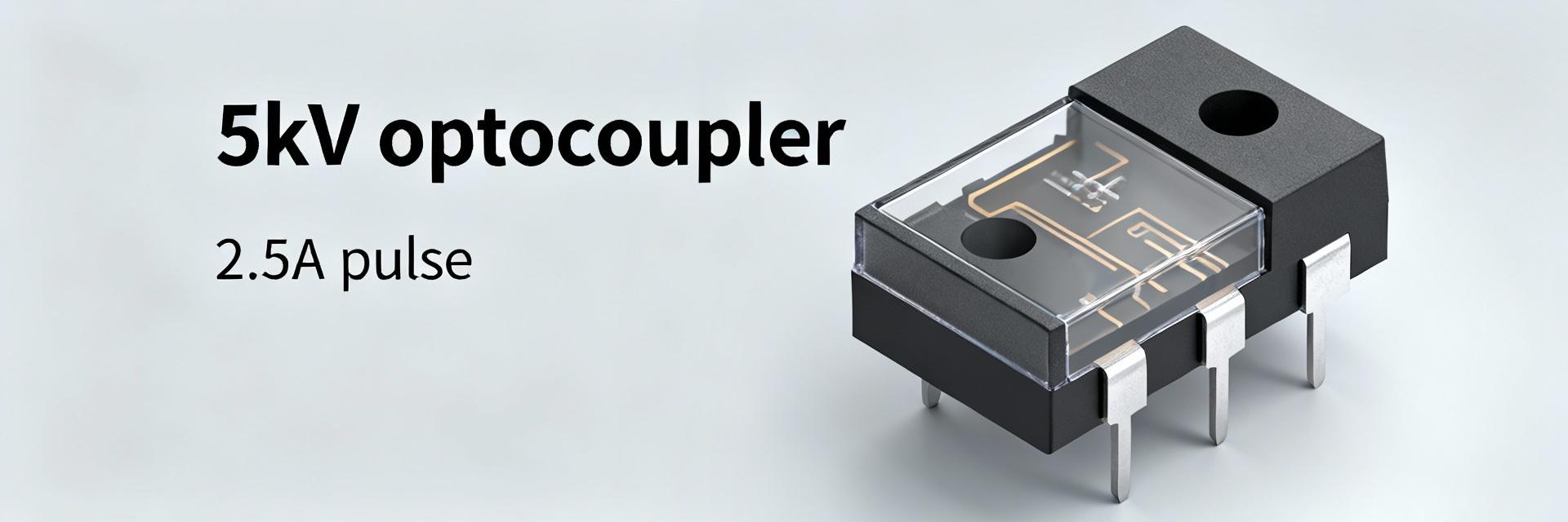
Point: The device combines high isolation with fast switching and strong peak drive. Evidence: rated 5 kVrms isolation, ~2.5 A peak output capability and sub-25 ns rise/fall behavior. Explanation: this article gives a practical, test-oriented examination of the optocoupler and its real-world performance for isolated gate-drive and control interfaces.
Background: Why this optocoupler matters for isolated gate drives (Background introduction)
Core function & target applications
Point: An optocoupler isolates low-voltage control from high-voltage power stages. Evidence: used in motor drives, inverters, industrial controls and telecom interfaces to transfer logic signals across safety barriers. Explanation: isolation prevents ground loops and protects controllers while allowing gate-drive signaling; designers prioritize isolation rating, drive capability and switching speed for reliable operation.
Isolation concepts & system-level implications
Point: Isolation rating affects PCB spacing and safety margins. Evidence: creepage/clearance rules and working vs. isolation voltage determine required keep-out and surge margins. Explanation: a 5 kVrms isolation rating raises allowable transient headroom, but designers must translate that into PCB creepage distances, insulation materials and decision points for spacing and conformal coating.
ACPL-K342-500E: Datasheet highlights & what each spec means (Data analysis / Specs)
Electrical & LED characteristics (input)
Point: Input LED parameters set drive requirements from controllers. Evidence: key values include maximum forward current, typical forward voltage and CTR or input-to-output coupling recommendations. Explanation: practical design uses MCU or level-shifter output, selects series resistor from Vf and desired If, and respects input timing limits to avoid thermal stress during pulsed operation.
Output, isolation & timing specs (output)
Point: Output specs determine switching performance and safe operating area. Evidence: highlight figures include ~2.5 A peak output, 5 kVrms isolation and rise/fall times near 22 ns plus propagation delay and thermal limits. Explanation: peak drive supports fast gate charging; rise/fall times and propagation delay govern switching loss and timing margins; thermal derating is needed for high duty or repeated pulses.
Performance benchmarks & test-driven insights (Data analysis / Performance)
Recommended lab tests and expected results
Point: A short bench test suite validates datasheet claims. Evidence: capture switching waveforms using defined CL/RL, measure rise/fall, propagation delay and pulsed output current under thermal monitoring. Explanation: expected benchmarks include sub-25 ns edges under light loading and verified 2.5 A short pulses; record tolerances and repeat tests at elevated ambient to expose derating behavior.
Robustness: ESD, surge and failure modes to watch
Point: Stress tests reveal common failure mechanisms. Evidence: overcurrent pulses, high dV/dt on outputs and sustained heating are typical stressors. Explanation: interpret outcomes by noting output saturation, timing shifts or permanent LED degradation; mitigate with series resistors, snubbers, current-limiting and improved heat spreading to prevent cumulative damage.
Design & integration guide: PCB, layout and circuit tips (Method / How-to)
PCB layout, creepage/clearance and grounding practices
Point: Layout enforces the isolation rating and signal integrity. Evidence: keep the isolation barrier free of copper, route low-inductance returns, and use stitching vias for safety ground zones. Explanation: set minimum keep-out, label silkscreen warnings, employ solder mask over slots where needed, and place input-side components away from high-voltage conductors to minimize coupling and improve testability.
Gate-drive circuit examples & passive component recommendations
Point: External components tailor drive strength and damping. Evidence: typical patterns use a series input resistor sized from Vf and If, pull-up/pull-down on output and gate resistors for MOSFET/IGBT switching. Explanation: choose snubber RC for dv/dt control, size gate resistor to trade switching speed versus overshoot, and account for package thermal limits in power-pulse scenarios for SO-8/SOIC handling.
Comparison & use-case scenarios (Case study / contextualization)
Trade-offs vs. other isolation approaches
Point: Optocouplers trade speed and simplicity against some integrated isolation alternatives. Evidence: optocoupler-based drives are compact, cost-effective and easy to route but require careful layout for higher-speed demands. Explanation: compared to transformers or capacitive isolators, they are often preferred for moderate-speed gate drives where simplicity and peak drive matter most.
Example application profiles
Point: Three short profiles show practical priorities. Evidence: (1) Three-phase motor inverter gate-drive needs fast edges and thermal margin; (2) industrial relay isolation emphasizes robustness and surge tolerance; (3) MCU-to-high-voltage sensor interface values creepage and noise immunity. Explanation: list top design considerations: switching losses, surge handling, and isolation spacing respectively.
Buyer's checklist & next steps for validation (Actionable recommendations)
Pre-purchase checklist
Point: Confirm mechanical, electrical and compliance fit before procurement. Evidence: verify package type/pitch, required isolation rating, supported output pulse currents, operating temperature range and generic safety certifications. Explanation: obtain samples for lot-to-lot checks, request recommended land pattern and reflow profile, and ensure procurement includes sample testing plans.
Validation plan before product launch
Point: Acceptance tests reduce field risk. Evidence: acceptance includes electrical bench tests, thermal cycling, isolation withstand and basic EMC assessments. Explanation: run repeatable test sequences, log propagation/timing shifts under stress, and compile datasheet, land pattern and application notes as part of final sign-off documentation for product release.
Conclusion (summary & SEO placement)
Point: The device blends high isolation with meaningful peak drive and fast switching for gate-drive use. Evidence: rated 5 kVrms isolation, strong pulsed output capability and fast edges support demanding interfaces. Explanation: realize intended performance only with deliberate PCB layout, component choices and bench validation to confirm in-system behavior.
Key summary
-
▸
High isolation with strong pulsed drive: device provides elevated transient headroom and ~2.5 A peak capability for short gate-charge events; designers must translate isolation rating into PCB spacing and insulation practice.
-
▸
Speed and thermal trade-offs: sub-25 ns edges enable fast switching but increase switching loss; thermal derating and pulsed current limits should guide duty-cycle and heat-spreading choices in layouts.
-
▸
Test-driven validation required: perform waveform capture, propagation delay and pulsed-current tests plus isolation withstand and thermal cycling to confirm real-world performance before production.
