The published datasheet for this device frames it as a two-channel logic-output optocoupler with a power output stage aimed at gate-drive and isolation tasks. Key headline numbers—approximately 0.4 A peak output drive, ~5 kV isolation capability, and sub-microsecond propagation—are the immediate pass/fail metrics you should verify when evaluating parts for IGBT/MOSFET drive.
This concise, spec-focused briefing highlights where to look in the datasheet, how to interpret limits, and which tests you should run. You will find actionable points on input LED drive, output supply and current rules, timing budgets, isolation practice, and a compact validation checklist tailored for fast prototype assessment.
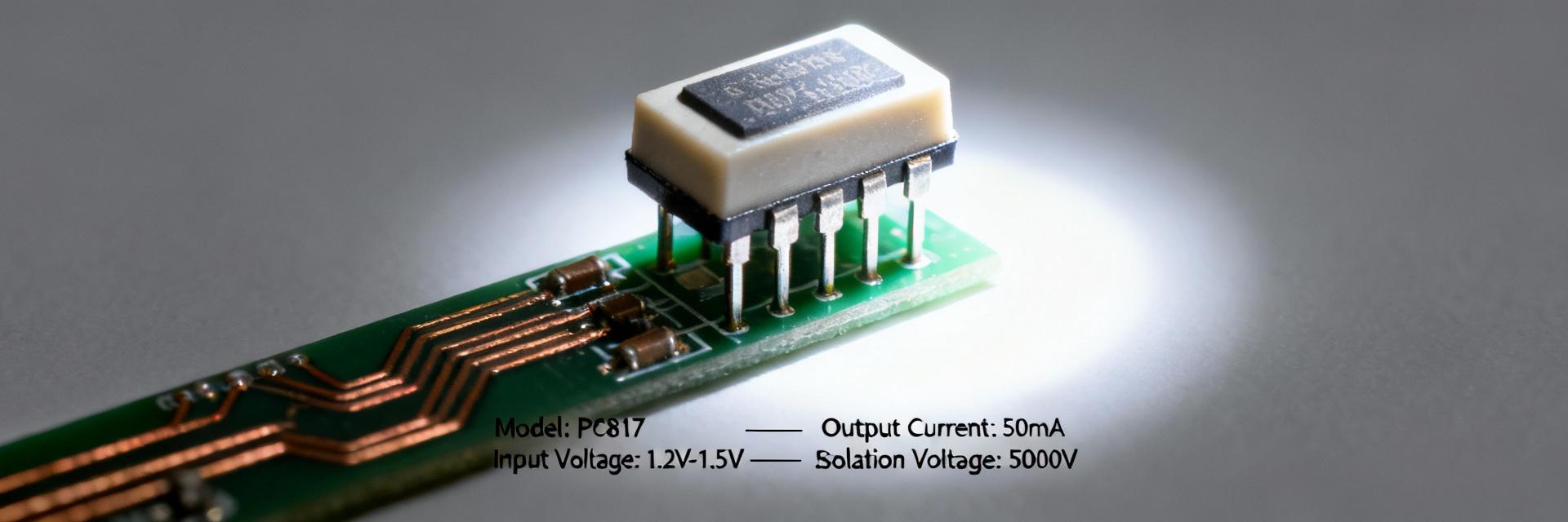
Quick Overview & Key Ratings (background)
What this device is and primary application
This device is a dual-channel optocoupler with integrated output drive intended for gate-drive isolation and level shifting. Typical applications include driving IGBT/MOSFET gates where galvanic isolation and transient immunity are required. Headline ratings from the published datasheet to call out: peak output current near 0.4 A, output-stage supply nominally 10–30 V, isolation voltage on the order of 5 kV, and propagation delay typically ~0.7 µs.
How to read the datasheet quickly
When you open the datasheet, follow this quick checklist: 1) absolute maximum ratings, 2) recommended operating conditions, 3) timing diagrams and test load conditions, 4) thermal limits and derating curves, and 5) isolation and safety tables. Also scan package/pinout and ordering codes for temperature grades so you match device variant to your application early.
Electrical Characteristics Deep Dive (data analysis)
Input LED and transfer characteristics
Input LED forward current and voltage determine recommended drive resistor and protection. The datasheet specifies typical If ranges and Vf; you should size series resistance to hold peak If below the absolute max while meeting the recommended If for reliable logic switching. Note transfer behavior: guaranteed logic thresholds and current-transfer behavior inform the minimum LED drive needed for consistent output margins across temp and lot.
Output stage: supply, output current, and voltage limits
The output stage VCC range is typically listed as a recommended window (for example, 10–30 V). The device provides a guaranteed peak output current in pulsed conditions around 0.4 A; continuous current limits are lower and must be respected to avoid thermal stress. Examine output saturation (VCE(sat) or equivalent) ratings—saturation voltage reduces effective gate-drive amplitude and must be included in your gate voltage budget.
Timing & Dynamic Specs (data analysis)
Propagation delay, rise/fall, and switching windows
Propagation delay figures typically list both turn-on and turn-off times with typical and maximum values; the published datasheet reports sub-microsecond typical delays that set deadtime and phase timing constraints in bridged converters. Rise and fall times affect how quickly gate charge is delivered and influence dV/dt immunity—slower edges can ease EMI but may increase switching losses.
Slew rate, switching limits, and recommended test conditions
Datasheet slew-rate or output transition slope is measured under specified load, VCC, and If; replicate these conditions to validate claimed timing. Maximum recommended switching frequency is driven by thermal dissipation and output-stage recovery; for pulsed gate currents, use the datasheet test conditions (load capacitance, pull-down/up load) to reproduce rise/fall and propagation metrics in your lab.
Isolation, Safety & Environmental Limits (method/guide)
Insulation voltage, RMS rating, and creepage/clearance considerations
An isolation rating around 5 kV and an RMS withstand voltage (e.g., 3750 VRMS) translate to PCB design rules: maintain adequate creepage and clearance, consider slotting or increased separation for high altitude or pollution degree environments, and apply conformal coating where contamination or humidity could reduce the effective standoff. Plan hipot and barrier testing per the datasheet limits.
Temperature, humidity, and reliability derating
Observe operating and storage temperature ranges and consult derating curves for output drive versus ambient. For elevated ambient or reduced airflow, reduce average output current or pulse duty to avoid junction overheating. Be mindful that humidity and long-term moisture absorption in the package can degrade insulation; qualification tests should include humidity-stress or bias-humidity as appropriate.
Design Guidelines & Common Pitfalls (method guide)
Driving the LED and matching driver stages
Select LED drive current to exceed the datasheet minimum for reliable logic output while staying below absolute maximum If. Use series resistors sized for worst-case Vf at low temperature, and add input protection (series resistor, transient clamp) to prevent overstress. Account for output saturation when setting gate-drive amplitude so the gate sees the intended VGE/VGS under load.
PCB layout, thermal management, and EMI mitigation
Keep input and output grounds separated and place output VCC decoupling capacitors close to the device pins. Provide thermal relief or copper pours to spread pulsed peak current heating and avoid hotspot or solder fatigue. Route to minimize common-mode coupling; use local RC snubbers or gate resistors consistent with the device's switching specs to control EMI and ring behavior.
Selection Scenarios, Test Checklist & Troubleshooting (case & action)
When this part fits (use-case matrix)
This part fits when you need high peak gate-drive current for short pulses, modest switching frequency, and a robust isolation barrier. If your design needs continuous high output current or multi-megahertz switching, consider alternatives. Use quick yes/no cues: output current ≥0.4 A pulsed = yes; propagation delay ≤1 µs = yes; isolation ≥5 kV = yes for high-voltage gate isolation.
Quick validation checklist and lab tests
Run these prototype tests: verify VCC range and output amplitude under worst-case load; measure propagation delays and rise/fall with intended gate capacitance; perform a hipot on the isolation barrier at the specified voltage; thermal soak with pulsed gate currents and monitor junction and board temps. Watch for LED overstress, thermal runaway, and unexpected output saturation during these tests.
