Introduction (data-driven hook — 10–15% of total words)
Point: The ATSHA204A-XHDA-T provides 256‑bit key strength, up to 16 key slots, a guaranteed unique 72‑bit serial number, a wide operating voltage range, and microamp sleep currents — numbers pulled directly from the datasheet and core specs to set expectations for engineers. Evidence: 256‑bit key length, 16 key slots, 72‑bit unique ID, low µA sleep current are the basis for design choices. Explanation: This article gives an engineer-focused interpretation of the ATSHA204A-XHDA-T datasheet, highlighting the specs to design against and practical integration guidance.
Background & Product Overview (background introduction)
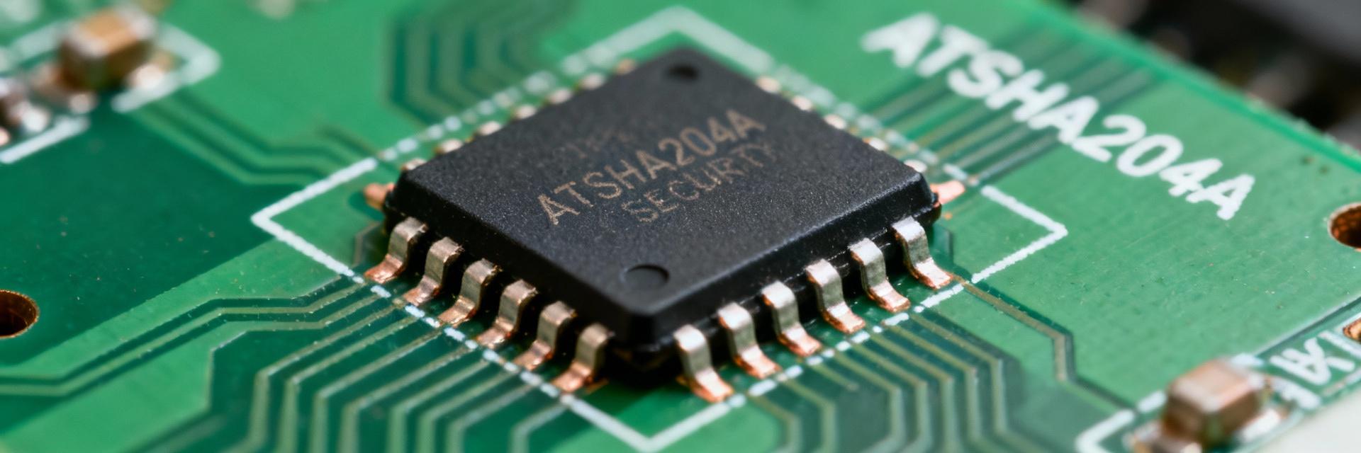
— What the ATSHA204A-XHDA-T is
Point: The ATSHA204A-XHDA-T is a dedicated authentication/security IC aimed at IoT, peripherals, and secure provisioning. Evidence: It implements hardware-based authentication primitives and secure non-volatile storage per the datasheet. Explanation: In practice it stores keys and performs challenge‑response and MAC operations, making it suitable for device identity, secure boot assist, and accessory authentication at low cost and power.
— Key differentiators at a glance (bullet list)
Point: Quick specs snapshot supports rapid evaluation. Evidence: Datasheet tables show these concrete values. Explanation: Use this scanable list to decide fit for your design.
- 256‑bit ECC‑level key strength (SHA‑256 based MACs)
- Up to 16 configurable key slots in EEPROM
- Guaranteed unique 72‑bit serial number per device
- Supported primitives: SHA‑256, HMAC/MAC, RNG, challenge‑response
- Low‑power modes with sleep currents in single‑digit µA
Key specs — visual snapshot
Note: bar lengths are illustrative relative indicators for quick comparison, not absolute performance graphs. Refer to the official datasheet for numeric tables used in design calculations.
Electrical & Absolute‑Max Specifications (data analysis)
— Power, voltage ranges, and current profiles
Point: Understanding operating voltages and currents is essential for battery designs. Evidence: The datasheet lists an operating supply range and absolute maximums, with active, idle and sleep current figures. Explanation: Choose a regulator that keeps the device within the recommended range; account for peak currents during crypto operations when sizing decoupling and regulator transient response. For battery systems, budget wake/sleep cycles against typical transaction currents.
— IO levels, timing constraints, thermal and reliability limits
Point: IO tolerances, ESD thresholds, and temperature ratings constrain system margins. Evidence: Datasheet tables specify recommended IO voltage levels, ESD protection ratings, and storage/operating temperature ranges. Explanation: Maintain IO within recommended bounds, add derating for thermal environments, and follow ESD handling procedures during assembly and test to protect the device and ensure lifetime reliability.
Cryptographic & Memory Specifications (data analysis)
— Keys, memory map, and secure storage
Point: Planning key allocation and provisioning is driven by the EEPROM layout and endurance. Evidence: The device exposes up to 16 key slots (256‑bit) and an EEPROM map with write/erase cycle limits in the specs. Explanation: Use one slot per device-unique secret for strongest isolation, reserve slots for firmware counters or configuration, and design provisioning flows to avoid excessive reprogramming due to EEPROM endurance limits.
— Supported primitives & authentication modes
Point: Cryptographic primitives and modes determine latency and protocol design. Evidence: SHA‑256, HMAC/MAC, and a hardware RNG are listed in the datasheet along with challenge‑response and MAC generation modes. Explanation: Expect single‑digit to low‑hundreds of millisecond latencies for operations depending on clocking and wake sequences; account for these in protocol timing budgets and host-side timeouts.
Communication & Integration Guide (method/guide)
— I2C interface, addressing, and timing (practical how‑to)
Point: Correct I2C signaling and wake/command sequencing are required for reliable operation. Evidence: The datasheet shows supported clock rates, ACK/NACK behavior and required wake token sequences. Explanation: For ATSHA204A-XHDA-T I2C timing, implement: idle → wake (special pulse) → send challenge → read response → sleep. Use conservative clock speeds initially, verify ACK/NACK patterns, and implement retry/backoff logic in host firmware.
— PCB footprint, hardware connections, and layout tips
Point: Layout and BOM choices affect noise immunity and reliability. Evidence: Application notes and recommended footprints in the datasheet give decoupling and land pattern guidance. Explanation: Place decoupling capacitors close to VCC pins, use proper pull‑ups sized to meet I2C rise time targets, keep traces short between host and device, and avoid routing noisy signals nearby to reduce EMI and ensure stable communications.
Reference Use Cases & Design Examples (case study)
— Example 1 — Secure key storage & device authentication (system flow)
Point: A common flow is provisioning unique keys and authenticating at boot. Evidence: The datasheet provides command sequences for write, challenge, and MAC verification. Explanation: Provision keys into secure slots during manufacturing, verify device identity via challenge‑response at first boot, and plan key rotation by reserving spare slots and implementing update procedures while respecting EEPROM endurance.
— Example 2 — Peripheral authentication & anti‑counterfeit
Point: The device can authenticate peripherals or accessories using a stored secret. Evidence: Challenge/response and MAC commands are designed for accessory validation. Explanation: Integrate a host check that sends a nonce and verifies returned MAC against expected logic; include test vectors and validation checklists to exercise edge cases and counterfeit detection scenarios during QA.
Implementation Checklist & Troubleshooting (actionable)
— Pre‑production checklist
Point: A concrete checklist reduces production surprises. Evidence: Datasheet tables identify ordering codes, package outlines, and electrical limits. Explanation: Verify ATSHA204A‑XHDA‑T ordering code and package, confirm voltage/current margins against regulator specs, perform footprint review, draft provisioning procedure, and create golden test vectors for manufacturing validation.
— Common issues & debugging tips
Point: Typical failures center on bus timing, power, and crypto parameter mismatches. Evidence: Observed symptoms map to datasheet timing and electrical constraints. Explanation: Use an I2C analyzer and oscilloscope to check wake pulses, ACK/NACK, and clock integrity; verify supply rails under load; confirm serial number readout to ensure unique ID accessibility and validate nonce/serial usage in MAC calculations.
Summary (10–15% of total words)
Point: Recap core device value and next steps. Evidence: Key specs such as 256‑bit keys, 16 key slots, 72‑bit unique serial, and low sleep current are central. Explanation: The ATSHA204A-XHDA-T delivers compact hardware authentication; use the datasheet to verify electrical and cryptographic limits and run the pre‑production checklist before prototype validation.
- The ATSHA204A-XHDA-T provides 256‑bit key capability and up to 16 EEPROM key slots; plan per‑device key allocation and provisioning to leverage secure storage and isolation.
- Electrical specs and current profiles in the datasheet drive regulator selection and decoupling choices; budget for wake and crypto peak currents in battery designs.
- Follow the I2C wake → challenge → response → sleep sequence and validate timing with an analyzer; include test vectors and serial number checks in manufacturing tests.
Call to action: obtain the official datasheet to cross‑check table numbers, execute the pre‑production checklist, and prototype the sample I2C challenge‑response flow in your lab.
