Point: This note summarizes the practical, measurable takeaways engineers need when evaluating a single‑lead biopotential front end: supply range, quiescent current, input/noise behavior, CMRR, and the chip’s role in ECG signal chains. Evidence: The breakout/module application schematics and the official datasheet present the reference circuits, electrical tables, and performance plots designers must validate on bench. Explanation: Readers will get a compact test and layout checklist plus pinout guidance to convert datasheet figures into repeatable board performance, with focused advice on the AD8232 pinout and where to double‑check the AD8232 datasheet for package specifics.
Background: What the AD8232 is and why it matters (background introduction)
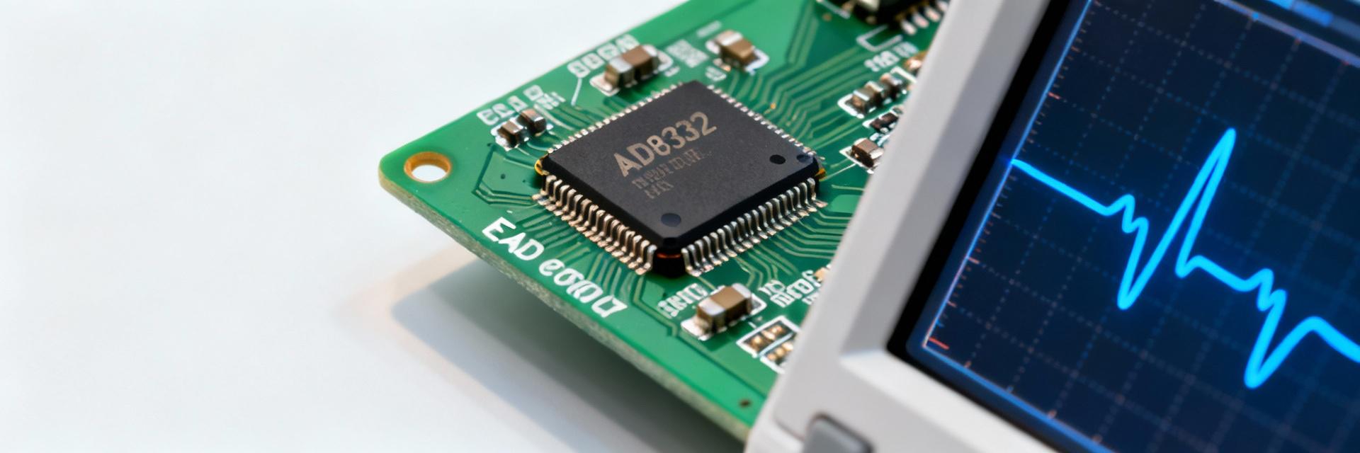
Intended applications and system role
Point: The device is optimized as a low‑power ECG front end for single‑lead heart‑rate monitoring and wearable biopotential front ends. Evidence: Reference application circuits show instrumentation‑amp input, right‑leg drive, reference handling and an output buffer feeding an ADC. Explanation: In a typical signal chain the chip sits directly after electrodes, providing initial amplification, common‑mode suppression and a conditioned output that an ADC or microcontroller samples for heart‑rate or waveform analysis.
High‑level functional blocks to watch in the datasheet
Point: Key internal blocks are the instrumentation amplifier, right‑leg drive (RLD), REF/driver op amp, and output filter stages. Evidence: Datasheet block diagrams and figure captions identify each block and recommended external components for gain and filtering. Explanation: Designers should map those blocks to layout and component choices: the INA sets gain and input matching, RLD improves CMRR for wearable leads, REF establishes mid‑rail and output bias, and output filtering defines ADC anti‑aliasing and baseline behavior.
Pinout overview & pin functions (background → pinout focus)
Pin map: pin names, numbers, and concise function descriptions
Point: Breakout modules and package variants expose pins such as power, ground, IN+, IN−, REF, RLD, OUTPUT, LO (leads off), and SHDN/SDN. Evidence: Typical module breakouts and datasheet pin tables list these names and recommended connections; common designer errors involve REF and RLD handling. Explanation: The following table shows a typical module pin mapping for fast prototyping—confirm chip package pin numbers in the official datasheet before PCB footprint work.
| Pin # (module) | Pin name | Short function | Recommended connection |
|---|---|---|---|
| 1 | 3.3V / VCC | Supply | Filtered 3.3V via local decoupling cap |
| 2 | GND | Return | Solid ground plane, nearby to VCC cap |
| 3 | OUTPUT | Conditioned signal | To ADC through filter; tie to REF for mid‑rail bias |
| 4 | IN+ | Non‑inverting input | Short trace to electrode; guard trace recommended |
| 5 | IN− | Inverting input | Short trace, matched impedance to IN+ |
| 6 | REF | Reference/mid‑rail | Decouple to ground; set ADC reference if required |
| 7 | RLD / RL | Right‑leg drive | Return to patient DRL electrode through low‑impedance path |
| 8 | SDN | Shutdown / lead detect | Pull to defined logic level per application |
Package variants and footprint notes
Point: The chip ships in multiple packages; pin numbers and land‑pattern details change per package. Evidence: Package drawings and mechanical tables in the datasheet provide toe, lead‑span, and pad recommendation figures. Explanation: Always confirm the package code on the order and cross‑check the land‑pattern tolerances; for small packages, maintain solder‑paste control and verify stencil aperture percentages to avoid tombstoning or insufficient fillet.
Datasheet performance summary: key electrical specs (data analysis)
Must‑check electrical specs and what they mean in practice
Point: Extract supply range, quiescent current, input‑referred noise, CMRR, input bias, gain range, common‑mode range, PSRR and output swing from the electrical tables. Evidence: These parameters determine battery life, achievable SNR, lead‑motion tolerance and ADC headroom per datasheet tables. Explanation: For wearables, prioritize low quiescent current and adequate CMRR; for diagnostic waveform fidelity, prioritize low input‑referred noise and enough output headroom to feed the chosen ADC without clipping.
| Spec | Typical / target | Practical impact |
|---|---|---|
| Supply range |
~2.0–3.5 V (confirm datasheet)
|
Determines sensor interface voltage and battery choices |
| Quiescent current |
~170 µA typical
|
Drives battery life in wearables |
| Input‑referred noise |
Low µV range (band dependent)
|
Affects SNR and P‑wave/QRS visibility |
| CMRR |
High dB (see datasheet plots)
|
Critical for rejecting mains and motion common‑mode |
Typical performance plots to reproduce and include
Point: Reproduce frequency response, input noise vs frequency, gain vs supply, and CMRR vs frequency from the datasheet. Evidence: Discrepancies between your plots and the datasheet often signal layout, component value, or measurement‑setup issues. Explanation: If noise is higher than expected, inspect input routing, shielding and reference decoupling; if CMRR falls off, validate electrode impedance balance and RLD loop integrity.
Recommended circuits & PCB layout best practices (method/guideline)
Typical application circuit explained step‑by‑step
Point: Follow the reference circuit: set INA gain with the recommended resistor network, AC‑couple per datasheet where needed, implement the RLD feedback, filter the OUTPUT and handle REF properly. Evidence: Datasheet reference schematics annotate critical resistor and capacitor values and tolerances. Explanation: Use precision resistors for gain setting, place AC coupling caps sized for desired low‑frequency roll‑off, and ensure the RLD amplifier sees a stable low‑impedance return to maintain CMRR.
PCB layout, grounding, and decoupling checklist
Point: Prioritize short input traces, local decoupling, and a single, solid analog ground near the device. Evidence: Layout recommendations in reference designs emphasize bypass capacitor placement and guard traces for IN pins. Explanation: Use 0.1 µF and 1 µF bypass caps adjacent to VCC; route IN+ and IN− as matched length, use guard traces tied to REF to reduce leakage, and keep RLD return path low impedance and separate from noisy digital returns.
Measurement & validation plan (data analysis + method)
Test setup: required instruments, fixtures, and test points
Point: Required gear includes a low‑noise power supply, signal/electrode simulator, differential probe, spectrum analyzer or high‑resolution ADC and shielded test fixture. Evidence: Datasheet measurement notes describe test conditions and recommended probe points. Explanation: Define test points at IN+, IN−, REF and OUTPUT; record SNR, input‑referred noise, CMRR, baseline wander and response under electrode motion to reproduce datasheet conditions and verify margins.
How to interpret results and common pitfalls
Point: Typical failure signatures are output saturation, elevated noise floor, and poor CMRR. Evidence: Datasheet limits give thresholds to compare; deviations point to layout or component errors. Explanation: If the output saturates, check supply rails, REF bias and gain resistor; if noise is high, inspect input routing and bypassing; if CMRR is poor, verify electrode balance and RLD loop connectivity.
Integration checklist & troubleshooting flow (action suggestions / case)
Practical integration checklist before first power‑up
Point: Verify power polarity, decoupling caps, populated gain resistor, proper REF decoupling, RLD connections, and correct footprint orientation. Evidence: Common pre‑power checklists in application notes reduce risk of immediate device failure. Explanation: Use the following quick checklist template on every board: power net polarity, VCC decoupling present, REF cap installed, gain resistor present, IN pin routes short, SDN defined, and board inspected for solder bridges.
Troubleshooting flow and corrective actions
Point: Prioritize checks: rails → ground/decoupling → gain network → inputs/electrodes → RLD. Evidence: Symptoms map to likely causes—saturation to bias/rail issues, noise to layout or missing caps. Explanation: Corrective actions include reinstalling bypass caps, swapping gain resistors, shorting inputs to known source to isolate, and temporarily disabling RLD to observe CMRR change.
Summary
Summary (expand/collapse)
Point: Converting datasheet figures into reliable product behavior requires focused checks on power, input handling, reference/RLD, layout, and measurement setup. Evidence: The pinout table and the spec highlights above represent the minimum items to validate against the datasheet. Explanation: Use the provided pin mapping as a prototyping guide, reproduce key plots in your lab, and follow the pre‑power checklist and troubleshooting flow to shorten debug time while preserving signal fidelity.
- Confirm the module pinout against the official package table and verify REF and RLD handling to protect CMRR and biasing.
- Validate supply range and quiescent current from the datasheet to size battery and estimate run time under target duty cycles.
- Reproduce frequency response and input‑referred noise plots in your test setup; deviations usually point to layout or probe errors.
- Follow a strict layout checklist: short IN traces, local decoupling, guard traces, and low‑impedance RLD return to minimize interference.
- Use the stepwise troubleshooting tree—rails, ground, gain network, inputs, RLD—to isolate failures efficiently.
