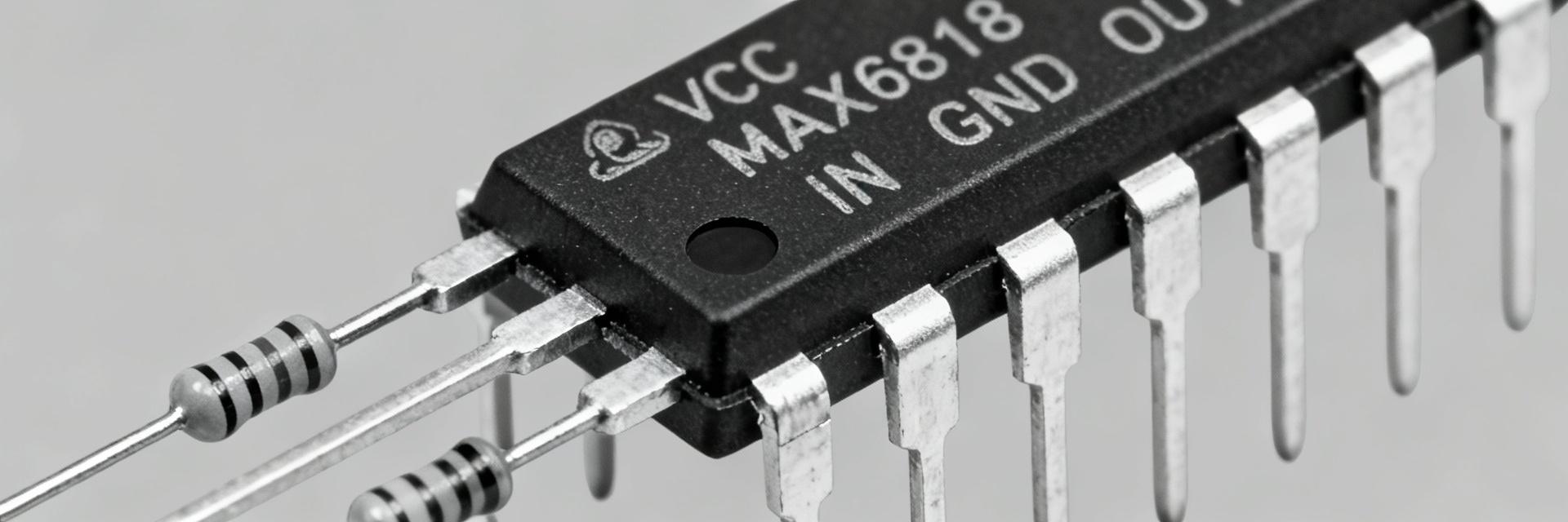
Point: The MAX6818 is an octal CMOS switch-debouncer/input interface optimized for low-power button and switch scanning; the MAX6818 datasheet highlights eight inputs, a typical supply range around 2.7–5.5 V, and robust ESD protection rated at ±15 kV on I/O pins. Evidence: Datasheet tables list per-pin ESD values and quiescent currents. Explanation: These numbers set expectations for interfacing to microcontrollers across common logic families while surviving industrial ESD events.
Point: This article maps practical details for design and validation. Evidence: Each H2 covers: product overview and headline specs; pinout and functional notes; electrical ratings and timing; integration and PCB best practices; test and procurement checklist. Explanation: Designers can use the sections as a quick reference when reading the official datasheet and preparing hardware bring-up.
Quick Product Overview & Key Specs (background) — 200–250 words
One-paragraph summary
Point: The MAX6818 is a CMOS octal switch debouncer and input interface intended for button and switch matrices and industrial I/O. Evidence: The datasheet describes single-chip debouncing with individual input thresholds, three-state outputs, and low standby current. Explanation: For embedded designs requiring compact front-end scanning and ESD robustness, the device consolidates multiple discrete components into a predictable, low-power interface.
At-a-glance spec table to include in the article
| Parameter | Typical / Range |
|---|---|
| Inputs | 8 (octal) |
| Supply Voltage | ~2.7–5.5 V |
| I/O Type | CMOS inputs, three-state or push-pull outputs |
| ESD Protection | ±15 kV (contact) |
| Operating Current | Low µA standby; mA active (datasheet typicals) |
| Package Options | SSOP-20 or equivalent |
| Temp Range | Industrial grade (see datasheet) |
Point: Designers should present this compact spec block prominently. Evidence: The datasheet calls out these headline numbers in the features and electrical summary. Explanation: A small visual callout with these specs accelerates design decisions and procurement checks.
Pinout & Functional Pin Descriptions (data analysis — pinout focus) — 250–300 words
Pinout diagram guidance & package variants
Point: Provide a labeled pinout for the chosen package, typically SSOP-20 or equivalent, showing grouped I/O, control pins, VCC, and GND. Evidence: The datasheet includes package pin maps and variant notes. Explanation: A clear pinout diagram helps PCB placement and silk-screening; highlight banks (inputs on one side, outputs on the other), VCC/GND pins, and any dedicated EN/OE or CH pins so engineers can quickly map signals to the board.
Pin-by-pin functional notes (recommended micro-sections)
Point: Break pins into groups with concise functional bullets. Evidence: Datasheet tables list thresholds, leakage, and recommended decoupling per power pin. Explanation: Example micro-sections: Inputs — CMOS-level thresholds, internal pull behavior, and ESD path; Outputs — drive type and three-state behavior; Control pins — active polarity for EN/OE and recommended tie-high/low; Power pins — VCC range and decoupling (0.1 µF + 1 µF near VCC); No-connects — mark on silk for manufacturability. Also suggest PCB silk annotations for each bank.
Electrical Specs & Ratings Deep-Dive (data analysis — specs focus) — 300–350 words
DC characteristics: supply, input/output limits, currents
Point: Prioritize supply range, logic thresholds, leakage and drive currents when reading the datasheet. Evidence: DC tables show min/typ/max for VCC, VIH/VIL, II/IO, and ICC. Explanation: For system compatibility, verify that the device’s VIH at 2.7 V meets your MCU logic high; check input leakage for high-impedance sensing and plan pull-ups/pull-downs accordingly. Use typical values for sizing decoupling but use max values for worst-case thermal and power budgeting.
AC/timing specs, ESD & absolute maximum ratings
Point: Read timing and absolute limits next: propagation delay, debounce windows, ESD, and absolute voltages. Evidence: The datasheet documents propagation delays, recommended debounce behavior, and ±15 kV contact ESD rating. Explanation: For debouncing, capture propagation and recommended input timing; respect absolute maximums by derating Vmax by ~10% in designs and add series resistors or input RC filters for surge protection. ESD margins inform protective TVS placement on exposed connectors.
Integration & Design Best Practices (method/guide) — 250–300 words
Typical application circuit & BOM notes
Point: A canonical schematic centers on VCC decoupling, input pull resistors, and EN/OE wiring. Evidence: Reference circuits in the datasheet show decoupling close to VCC and example pull networks. Explanation: Recommended BOM items: 0.1 µF ceramic at VCC, 1 µF bulk, 10 kΩ pull-ups for switch inputs, optional 100 Ω series resistors for high-speed lines. Tie unused inputs per datasheet guidance to avoid floating states.
PCB layout, grounding, and EMI/ESD protection tips
Point: Layout is critical: place decoupling next to VCC pin(s), use short traces for sensitive inputs, and route ground returns with vias. Evidence: Datasheet reliability notes and application tips emphasize decoupling placement and ESD behavior. Explanation: For EMI/ESD, place TVS diodes or series resistors close to connector pins rather than the device; add ground stitching via under the package and avoid routing noisy power traces under input traces. Search phrase to include: "MAX6818 PCB layout tips".
Testing, Troubleshooting & Selection Checklist (case/action) — 200–250 words
Test procedures & common failure modes
Point: Follow bench tests: continuity, power sequencing, input toggle, and quiescent current. Evidence: Datasheet recommends measuring ICC and timing to verify debouncing. Explanation: Test steps: verify VCC and GND continuity; power device and measure standby current; apply button stimulus and capture input vs output on an oscilloscope to observe bounce vs debounced output; measure propagation delay. Common failures: missing decoupling, floating EN/OE, or ESD-damaged pins.
Procurement, compliance & alternative selection criteria
Point: Procurement should confirm package, temp grade and lifecycle status. Evidence: Datasheet and reliability notes list footprint and temperature options. Explanation: Checklist: match channel count and VCC range, verify ESD rating, confirm pin compatibility for replacements, and test samples on an eval board. Reference the official datasheet when qualifying parts in your BOM.
Summary & Next Steps (100–150 words)
Point: The MAX6818 datasheet condenses key design drivers: pinout mapping, supply and timing specs, and robust ±15 kV ESD protection. Evidence: Headline tables and example circuits in the datasheet support these conclusions. Explanation: For next steps, download the official datasheet PDF, create a one-page pinout/summary for the PCB team, assemble the recommended reference circuit on an evaluation board, and run the oscilloscope debouncing test to validate behavior under real switches.
