The following deep dive frames relevance using key datasheet highlights: the LM1458N is a legacy dual op amp with a gain‑bandwidth product on the order of 1 MHz, quiescent supply current of a few milliamps per package, input‑bias currents in the hundreds of nanoamperes, and an operating supply range roughly from ±3 V to ±18 V (6 V to 36 V total). These practical numbers explain why designers select it for basic audio stages and general‑purpose signal conditioning.
This article unpacks the datasheet — pinout, electrical DC/AC behavior, application notes, PCB tips and troubleshooting — so engineers can interpret spec tables, predict real‑world behavior, and avoid common pitfalls when deploying the device in prototypes and production.
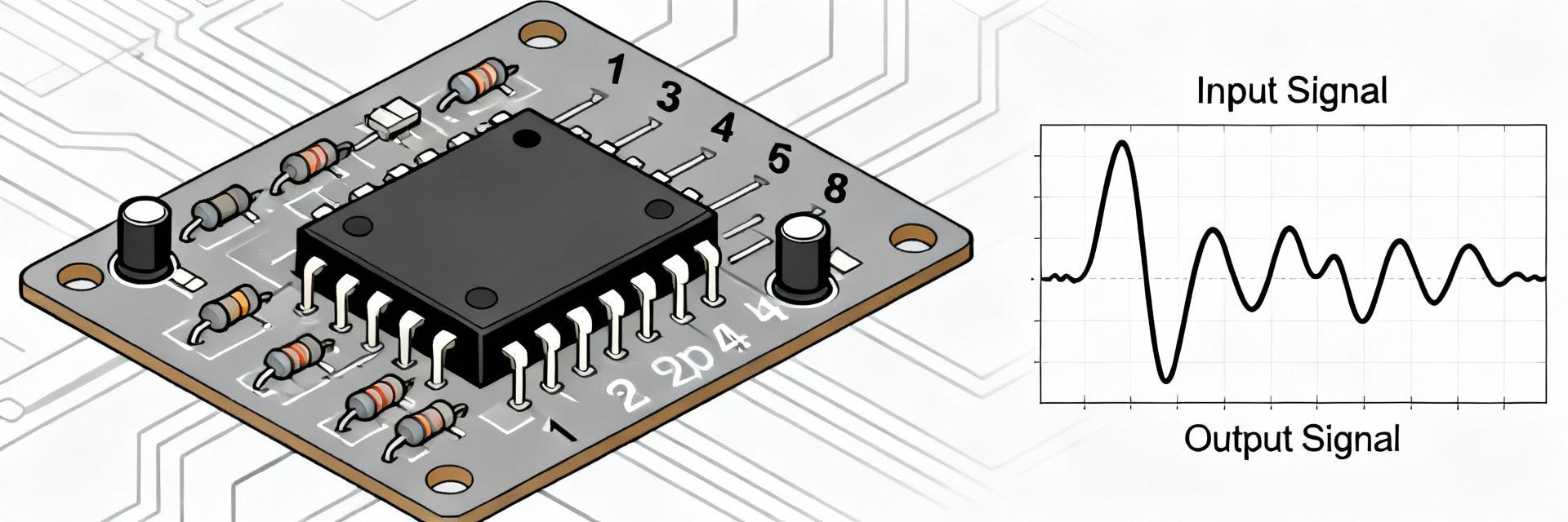
LM1458N at a Glance: Part Function, Packages & Pinout (background introduction)
Pinout & Pin Functions
Point: The LM1458N is a dual operational amplifier packaged commonly in 8‑pin DIP or SOIC, with each amplifier sharing the same supply rails. Evidence: Standard pin mapping lists V+ and V− on opposing pins, with two sets of inputs (In+, In−) and outputs (Out) for channels A and B. Explanation: Typical pin numbering for DIP‑8 places V+ at pin 8 and V− at pin 4; pins 1–7 map to In/Out for the two amplifiers, so designers must confirm orientation to avoid reversed rails or swapped channels when placing the IC.
Package Variants & Mechanical Notes
Point: Multiple package options affect footprint and thermal behavior. Evidence: Common variants include PDIP‑8 and SOIC‑8; some sources list small‑outline or plastic DIP bodies with the same electrical pinout. Explanation: For PCB layout, choose the package matching your assembly capabilities; DIP offers easy breadboard use while SOIC saves board area. Account for lead spacing, maximum package temperature and solder‑reflow profiles when specifying footprint tolerances.
| Package | Code | Footprint Note |
|---|---|---|
| PDIP-8 | DIP | 0.300" spacing; through‑hole; prototyping friendly |
| SOIC-8 | SOIC | 4.9 mm body; 1.27 mm pin pitch; surface mount land pattern |
DC Electrical Characteristics: What the Datasheet Actually Means (data analysis)
Input & Output DC Specs (Vos, Ib, Ios, Input Range, Output Swing)
Point: DC specs define precision and headroom. Evidence: The LM1458N shows input offset voltages in the low‑millivolt range, input‑bias currents in the hundreds of nanoamperes, and output swing limited to within a volt or two of the rails on typical loads. Explanation: For precision DC work, offset and bias current matter; consider offset trimming or alternative amplifiers for millivolt‑level accuracy. For single‑supply use, derate expectations — output cannot reach the rails, so plan headroom accordingly.
| Parameter | Typical / Practical Value |
|---|---|
| Input offset (Vos) | Low mV range — expect up to several mV |
| Input bias (Ib) | Hundreds of nA |
| Quiescent current (Iq) | Few mA per package |
| Supply range | ≈ ±3 V to ±18 V (6–36 V total) |
Supply, Quiescent Current & Thermal Limits
Point: Supply and thermal limits govern reliability. Evidence: Quiescent current multiplies by ambient and package thermal resistance to determine junction temperature under load. Explanation: Estimate junction temperature using Pd = (V+ − V−) × Iq plus dynamic dissipation; select bypass capacitors and ensure adequate copper to spread heat. Use 0.1 µF local decoupling close to supply pins to stabilize operation and reduce supply‑induced distortions.
AC Performance & Frequency Behavior (data analysis / methods)
Open‑Loop Gain, Gain‑Bandwidth, and Slew Rate
Point: AC specs set usable closed‑loop bandwidth and transient limits. Evidence: With a gain‑bandwidth around 1 MHz and a modest slew rate (sub‑1 V/µs, typical example ≈0.5 V/µs), the amplifier supports audio and low‑frequency filtering but not high‑speed signals. Explanation: For a target closed‑loop bandwidth, divide GBW by desired bandwidth to get maximum closed‑loop gain. Example: to achieve 20 kHz bandwidth, closed‑loop gain should be ≤50 (1 MHz / 20 kHz = 50), so a gain of 40 is practical; monitor slew limits for large‑amplitude, fast edges.
Noise & Stability / Compensation Notes
Point: Noise floor and capacitive loads affect stability. Evidence: The device is not a low‑noise specialist; stability can degrade with large capacitive loads on the output. Explanation: Use small series resistors (10–100 Ω) at outputs to isolate capacitive cables or filter caps, and run AC tests with the same bypassing and loads used in application when comparing to datasheet curves. Proper power‑rail decoupling and short ground returns improve measured noise and stability.
Typical Applications, Reference Circuits & PCB Layout Tips (case + methods)
Common Application Circuits
Point: Canonical circuits include inverting, non‑inverting and simple audio preamp topologies. Evidence: An inverting stage with Rf=10k and Rin=1k yields gain −10 and bandwidth ~100 kHz in practice; a non‑inverting buffer with gain 5 (Rf/Rg = 4) is common for level shifting. Explanation: For audio preamps, pick resistor values to balance noise (higher values increase thermal and bias‑current induced errors) against loading; add input coupling caps and output DC blocking caps where single‑supply operation is used.
PCB Layout, Decoupling & Reliability Tips
Point: Layout strongly affects performance and stability. Evidence: Short supply traces and a 0.1 µF ceramic close to the supply pins reduce rail impedance at audio and RF frequencies. Explanation: Checklist — place 0.1 µF decouplers within 2–3 mm of pins, add 10 µF bulk near regulator, use ground plane, route inputs away from digital switching, and include series output resistors when driving capacitive loads. For production, add test points for rails and inputs to simplify debugging.
- 0.1 µF ceramic + 10 µF bulk per supply
- Short traces from decoupler to pins; ground plane underneath
- Series output resistor for capacitive loads; guarded analog inputs
Troubleshooting, Selection Alternatives & Quick Design Checklist (action recommendations)
Common Failure Modes & Troubleshooting Steps
Point: Typical issues include output saturation, oscillation and unexpected offset. Evidence: Saturation often follows violated input common‑mode or insufficient supply headroom; oscillation correlates with poor decoupling or capacitive loading. Explanation: Troubleshooting steps — verify rails at the package, measure input common‑mode voltages against datasheet limits, temporarily add a 100 Ω series resistor at the output to quench oscillation, and swap in a known good device to rule out damage.
When to Choose a Different Op Amp & Selection Criteria
Point: The LM1458N is fine for basic audio and general tasks but not for precision or high‑speed needs. Evidence: If you need lower offset, lower noise, higher GBW or rail‑to‑rail outputs, the datasheet metrics to compare are Vos, input noise density, GBW and output swing specs. Explanation: Quick decision table below helps map requirement to the priority spec to search for in alternatives.
| If you need… | Prioritize in datasheet |
|---|---|
| Low offset / DC accuracy | Vos, input offset drift, offset trim |
| Higher bandwidth | GBW, open‑loop gain vs frequency |
| Drive to rails | Output swing, rail‑to‑rail spec |
Key Summary
- The dual amplifier pin configuration maps two full op amps to an 8‑pin package; confirm pinout before insertion to avoid reversed rails and swapped channels.
- The most critical datasheet checks are supply range, input bias/offset characteristics, gain‑bandwidth and output swing — these dictate precision and headroom.
- For audio use, expect ~1 MHz GBW and modest slew rate; choose closed‑loop gain to fit GBW and add output isolation for capacitive loads.
- PCB rules: place 0.1 µF decouplers at pins, use a ground plane, and include series resistors for stability when driving capacitive loads.
FAQ
What are the typical supply limits for LM1458N?
Answer: The device operates over a wide total supply span, commonly used from roughly 6 V total up to about 36 V total (±3 V to ±18 V rails). Always check the datasheet absolute maximums and plan headroom so outputs and inputs remain within the specified common‑mode and output swing ranges.
How can I stop oscillation or instability in audio circuits?
Answer: Tighten decoupling with a 0.1 µF ceramic at the supply pins, keep input traces short, add a small series resistor (10–100 Ω) at the output to isolate capacitive loads, and verify the layout follows a continuous ground plane. Reproduce datasheet test conditions when characterizing AC behavior.
What quick bench checks verify basic DC health of the amplifier?
Answer: Verify supply voltages at the package, measure quiescent current per package to confirm it matches expected few‑mA range, check that inputs sit within the common‑mode window, and confirm outputs are not pinned at rail; these steps isolate supply, input range and output‑stage problems efficiently.
