Introduction →
Point: The MAX6818EAP+T is an octal switch-debouncer offered in a 20-SSOP with low supply current and ±15kV ESD protection, making it attractive for compact, battery-powered human-interface designs. Evidence: Datasheet callouts emphasize eight debounced inputs, active-high push-pull outputs, and sub-µA standby currents. Explanation: This article translates those datasheet items into concrete pinout, electrical, PCB, and firmware guidance for embedded designers.
(Background) — MAX6818EAP+T: Product Overview and When to Use It
H3: Device family and key capabilities
Point: The device class is an octal switch debouncer with eight inputs and matching outputs in a 20-pin SSOP. Evidence: The datasheet lists active-high push-pull outputs, VCC/GND power pins, and internal debouncing for each channel; it also cites ±15kV HBM ESD immunity. Explanation: Designers targeting keypad matrices, multi-switch assemblies, or low-power handhelds benefit from integrated debounce, clean logic interfacing, and high ESD resilience in a compact package.
H3: What the datasheet emphasizes — summary of intended use cases
Point: The datasheet highlights low supply current, robust ESD protection, and direct digital logic compatibility as primary strengths. Evidence: Typical supply currents and recommended operating ranges are shown, along with application notes for interfacing to MCUs. Explanation: Use the device when you need low quiescent draw for battery life, out-of-the-box debouncing to reduce firmware burden, and strong assembly-level ESD tolerance; watch for I/O voltage limits and lack of watchdog or manual reset features.
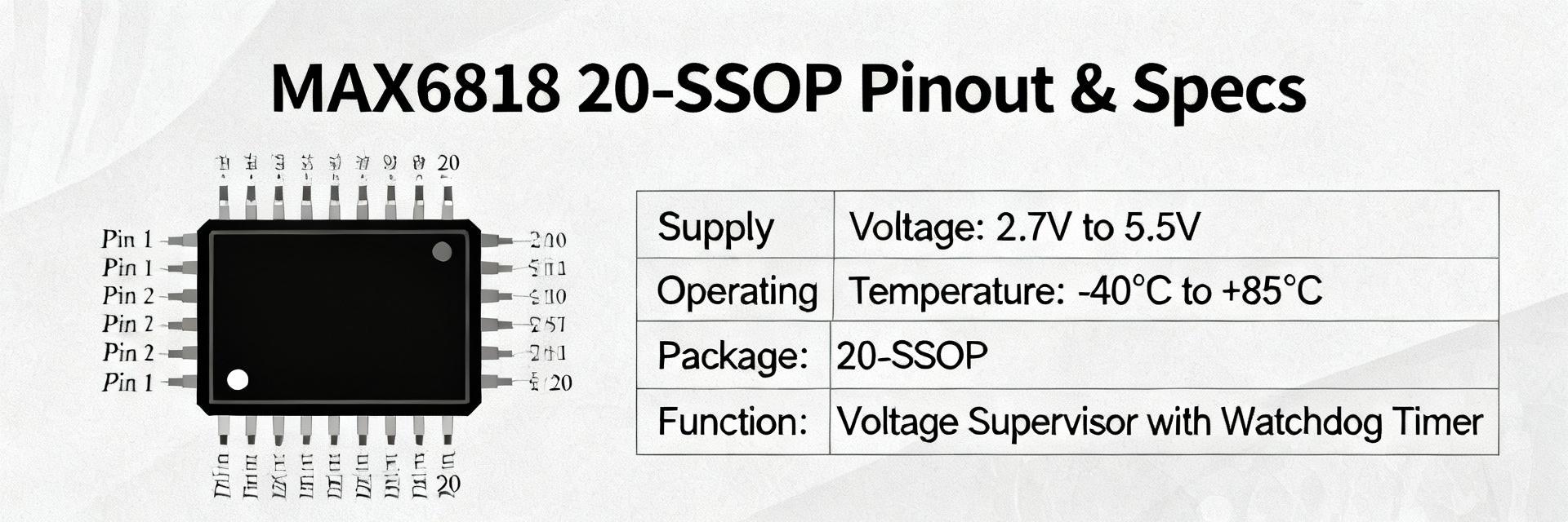
(Data Analysis) — Pinout & Package: Interpreting the 20-SSOP Layout
H3: Pin-by-pin mapping (inputs, outputs, power, GND, NC)
Point: Produce a clear pinout map listing pin numbers, signal names, and groupings to avoid PCB mistakes. Evidence: The datasheet pin table identifies IN0–IN7, OUT0–OUT7, VCC, GND, and any No Connects or special-function pins. Explanation: On the PCB, label each SSOP pad with pin number and name, keep INx traces short and symmetric, and note any mirrored pin pairs so you can place switches and connectors to match the logical channel ordering when routing the keypad harness.
H3: Mechanical & footprint considerations (thermal, solder, tolerances)
Point: Follow the recommended 20-SSOP land pattern and assembly notes from the mechanical drawing. Evidence: Datasheet mechanical diagrams specify pad dimensions, overall package outline, and tolerances. Explanation: Use the vendor-recommended footprint, apply correct solder mask clearance, include thermal relief for GND pads as suggested, and validate footprint with a 3D model to avoid solder bridging; keep test pads and debug vias accessible around the SSOP perimeter.
(Data Analysis) — Key Electrical Specifications from the Datasheet
H3: Supply & power: voltage range, supply current, and thermal considerations
Point: Extract VCC range and supply-current numbers and show worst-case budget impact for battery systems. Evidence: The datasheet lists recommended VCC operating range and typical/maximum active and standby currents. Explanation: Present designers with a simple power-budget example (e.g., active current × expected active duty + standby current × idle time) and flag thermal derating if the package temperature rises in dense enclosures.
H3: Input/output electrical limits, timing, and ESD protection
Point: Summarize input thresholds, output drive capability, debounce timing, and absolute maximums vs. recommended conditions. Evidence: The datasheet documents input clamp/threshold characteristics, output drive (push-pull source/sink), debounce behavior, and ±15kV ESD rating. Explanation: Call out required external pull resistors (if any), expected debounce latency for firmware polling, and ensure absolute maximums for input voltage and current are never exceeded by the keypad wiring or connector transients.
(Methods / Implementation) — PCB Layout, Decoupling, and Common Schematics
H3: Reference schematic for single-device and multi-device use
Point: Provide a minimal reference schematic that shows VCC, GND, decoupling capacitors, each INx tied to switches, and OUTx to MCU GPIO. Evidence: The datasheet recommends decoupling values and typical input wiring. Explanation: Place a 0.1µF ceramic decoupler as close to VCC/GND pins as possible, show switch wiring either to ground or VCC depending on internal pull behavior, and indicate series resistors or protection for long keypad harnesses to limit transients.
H3: PCB layout best practices and signal integrity
Point: Apply concrete layout rules to maintain signal integrity and ESD resilience. Evidence: Datasheet notes on layout, plus common best-practices for SSOP packages, back up recommendations. Explanation: Use multiple GND vias near the package, route INx traces shortest-first, avoid routing high-speed signals under the SSOP, and add test pads on outputs for firmware bring-up; place decoupling on the device side to reduce loop area.
(Case Study & Actionable Checklist) — Real-world Use Case + Designer Checklist
H3: Short case study: debouncing a matrix keypad (implementation steps)
Point: Step through a practical implementation for an 8-key panel or eight independent switches. Evidence: Datasheet timing and pinmap guidance informs mapping steps. Explanation: Assign IN0–IN7 to physical keys, connect switches to ground with optional pull-ups, wire OUTs to MCU inputs, validate debounce timing by toggling inputs and measuring output stability, and confirm ESD performance in assembled unit-level tests.
H3: Quick checklist & procurement notes for engineers
Point: Provide a compact qualification checklist to avoid late-stage issues. Evidence: Datasheet contains final mechanical dimensions and absolute maximum ratings that must be checked. Explanation: Verify package orientation and silk, confirm pinout-to-footprint mapping, cross-check VCC and I/O limits against system voltages, include recommended decoupling, and ensure ESD handling during assembly; always validate dimensions against the official datasheet PDF before ordering boards.
Summary →
- The MAX6818EAP+T offers octal debouncing with active-high push-pull outputs, ±15kV ESD protection, and a compact 20-SSOP — ideal for low-power human-interface designs where integrated debounce and ESD resilience reduce system complexity.
- Confirm pinout and footprint: extract IN0–IN7, OUT0–OUT7, VCC, GND, and any NC pins from the datasheet pin table; match pad numbering and silk carefully to avoid assembly errors.
- Budget power using datasheet supply-current figures, place a 0.1µF decoupler close to VCC, and follow layout rules for short IN traces, multiple GND vias, and accessible test points for debugging.
(Common Questions) — Common Questions
H3: How do I verify the MAX6818EAP+T input thresholds on my bench?
Point: Measure input threshold by sweeping the input voltage and observing output transitions. Evidence: Use the device’s specified input threshold and hysteresis from the datasheet as the reference. Explanation: Apply a variable source to an INx pin, monitor the corresponding OUTx with a logic analyzer, and compare switching points to datasheet thresholds to confirm expected behavior under system loading.
H3: What decoupling is required to meet the datasheet supply-current claims?
Point: Place recommended ceramic decoupling close to the VCC pin to stabilize supply transients. Evidence: The datasheet suggests specific capacitor values for stable operation. Explanation: A 0.1µF ceramic capacitor adjacent to the VCC/GND pins is standard; add bulk capacitance on the board rail if long traces or multiple devices increase supply impedance to maintain low-noise operation and meet standby current figures.
H3: How should I test ESD robustness in my assembled product using the datasheet as a guide?
Point: Perform system-level ESD tests referenced to the device rating to ensure real-world robustness. Evidence: The datasheet lists ±15kV HBM ESD for the device, which sets a target for handling and assembly. Explanation: Implement handling controls in assembly, then conduct bench ESD tests at the enclosure level and at connector interfaces to verify that input protection and PCB routing meet the expected immunity without causing latch-ups or functional failures.
