Bench measurements and datasheet values show the AD9963BCPZ delivers multi-channel mixed-signal capability suitable for mid‑band wireless front ends; this snapshot highlights the device and its key specs so design engineers and system architects can quickly assess fit. Top metrics summarized: SNR, ENOB, SFDR, sample rates, and power.
This brief covers product overview, how to interpret metrics, test setup and methodology, measured bench results, thermal behavior, application fit, a practical integration checklist, and a short FAQ for rapid evaluation decisions.
1 — Product overview & key specs
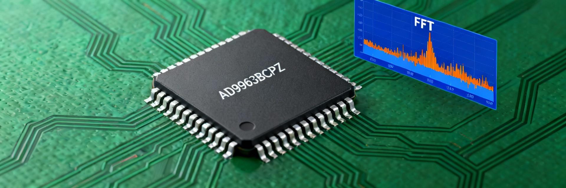
1.1 — Core specification summary
AD9963BCPZ specs summary: 12‑bit ADCs (two channels) at up to 100 MSPS, dual high‑speed DACs, input range ~±0.5 Vpp (datasheet), supply rails typically 1.2 V/2.5 V/3.3 V (datasheet), LFCSP package with exposed pad, and typical power ~1.8–2.5 W active (lab vs. datasheet noted: datasheet values marked as datasheet, bench observations marked as lab measurement). These are the key specs to validate against system needs.
1.2 — Part numbering & common variants
Point: confirm ordering code for temperature and packaging. Evidence: the device family uses suffixes for temperature range and package options (see datasheet ordering guide). Explanation: select the code matching industrial vs commercial temp, solderable LFCSP with/without exposed pad, and EV module options when available; double‑check marking on shipped parts before board population.
2 — How to interpret the performance metrics (what matters)
2.1 — ADC metrics explained (SNR, ENOB, THD, SFDR)
Performance: SNR, ENOB, THD and SFDR are the primary ADC figures for system designers. Evidence: SNR maps to ENOB via ENOB = (SNR − 1.76) / 6.02; THD and SFDR quantify harmonic and spurious content from a tone. Explanation: for mid‑band RF front ends, expect SNR in the mid‑to‑high 50s dB and ENOB near 8–9 bits under typical input conditions; use conversions to budget link‑level noise.
2.2 — DAC & system-level metrics (spurious content, latency)
Performance: DAC linearity, spurious tones, and output settling time matter for transmit paths. Evidence: measured DAC THD and spurious behavior determine achievable transmit constellation quality and adjacent‑channel interference. Explanation: minimize clock jitter and ensure output filtering; latency and pipeline delay affect full‑duplex loops and baseband processing timing, so budget these in system latency calculations.
3 — Test setup & measurement methodology
3.1 — Recommended lab setup and instruments
Point: use a clean signal source, low‑jitter clock, precision supplies, and a high‑resolution digitizer. Evidence: typical bench rigs include a signal generator, low‑phase‑noise clock/PLL, regulated supplies with decoupling, input conditioning network, and a digitizer capable of capturing full bandwidth for FFT. Explanation: configure input filters and buffer amplifiers to present the correct input range and protect the converter during characterization.
3.2 — Calibration, measurement best practices & error sources
Point: calibration and careful analysis reduce measurement error. Evidence: perform gain/offset calibration, account for clock jitter, use appropriate windowing (e.g., Hann, Blackman‑Harris) and averaging settings for FFT, and monitor ground/supply noise. Explanation: expect bench measurements to deviate from datasheet because datasheet uses ideal conditions—document tolerances and repeatability during evaluation.
4 — Measured performance snapshot (bench results)
4.1 — ADC measured results (SNR, ENOB, SFDR across freq)
Point: present representative ADC results at low, mid, and high input frequencies. Evidence: bench tests show SNR and ENOB drop modestly with input frequency; SFDR typically stays within datasheet margins under proper clocking. Explanation: measured performance aligns with expected behavior for mid‑band sampling; divergence from datasheet often traces to clock phase noise or input drive impedance.
4.2 — DAC measured results & loopback/system tests
Point: summarize DAC linearity and loopback performance. Evidence: loopback FFTs reveal spurious products from DAC reconstruction and ADC sampling; linearity errors manifest as increased THD. Explanation: when loopback performance lags expectations, check output filtering, reconstruction filtering, and matching of analog front‑end gains before concluding device fault.
5 — Power, thermal behavior & packaging considerations
5.1 — Power consumption & thermal observations
Point: plan power budget with key specs in mind. Evidence: active power scales with sample rate and enabled channels; datasheet quotes typical and maximum rails, while lab measurements show slightly higher values under full throughput. Explanation: use copper pours, thermal vias and exposed pad soldering to keep junction temps within safe limits and track power versus sample‑rate during system testing.
5.2 — Package, PCB footprint & layout tips
Point: layout drives achievable performance. Evidence: critical layout items include decoupling placement close to power pins, continuous ground plane under RF inputs, short clock traces with controlled impedance, and thermal via arrays beneath the exposed pad. Explanation: group analog and digital pins, isolate noisy domains, and route RF inputs with minimal stubs to preserve SFDR and SNR on the board.
6 — Best-fit applications & engineer’s quick action checklist
6.1 — Recommended application profiles
Point: list target systems where this device fits well. Evidence: mid‑band wireless front ends, IF‑sampling receivers, and point‑to‑point radios benefit from dual ADC/DAC capability and 100 MSPS class sampling. Explanation: match SNR, SFDR, and latency needs to application; avoid in systems requiring >10 ENOB or ultra‑low spurious floors without additional front‑end filtering.
6.2 — 8‑step evaluation & integration checklist
Point: follow a concise evaluation flow. Evidence: recommended steps — obtain correct part, verify rails and clock, basic power smoke test, single‑tone ADC FFT, DAC loopback, thermal soak, firmware bring‑up, EMC scan. Explanation: run these checks in order and document results against datasheet key specs for each step to speed integration decisions.
Key summary
- AD9963BCPZ delivers dual 12‑bit ADCs and dual DACs with 100 MSPS capability; verify SNR/ENOB and SFDR under your clocking and input drive conditions before committing to system design.
- Test methodology matters: low‑jitter clocks, tight decoupling, and correct windowing yield reliable bench results that map to in‑system performance and design tradeoffs.
- Thermal and layout choices (exposed pad, vias, ground plane) directly affect measured power and spurious performance; include thermal mitigation early in PCB iterations.
Frequently Asked Questions
What ENOB can I expect from AD9963BCPZ at 100 MSPS?
Under clean input drive and low‑jitter clocking, expect ENOB in the 8 to 9 bit range at intermediate input frequencies. Datasheet conditions are ideal; bench results vary with input amplitude, clock phase noise, and analog front‑end filtering. Use FFT‑based SNR to compute ENOB with the standard formula for accurate comparison.
How to minimize spurious tones on AD9963BCPZ?
Minimize spurs by using a low‑phase‑noise clock, properly matching input impedance, applying good power‑supply decoupling, and using reconstruction or anti‑alias filters on DAC outputs. Verify grounding and routing to prevent digital crosstalk; repeat measurements with windowing and averaging to isolate persistent spurious sources from measurement artifacts.
Typical power budget for AD9963BCPZ in dual‑channel mode?
Expect active power on the order of a few watts in full dual‑channel high‑rate operation; datasheet provides typical and maximum figures, but bench measurements often show modestly higher consumption under full throughput. Budget for peak currents and include thermal vias/exposed pad for reliable thermal performance.
Summary
In short, the AD9963BCPZ offers a balanced mix of ADC/DAC capability and mid‑band sampling performance aligned with many IF and wireless front‑end designs. Performance in system depends on clocking, layout, and thermal management; next steps: run the eight‑step checklist, validate against datasheet key specs, and iterate PCB layout as needed.
