The KSZ8995MA datasheet lists dozens of electrical parameters that directly determine board power budget, signal-integrity margins, and PHY timing compliance — any one mis-read value can cost weeks in debug. This introduction highlights why designers must extract the KSZ8995MA datasheet values for power rails, I/O limits, thermal constraints, and timing before a first PCB spin.
Point: Begin with a data-driven reading strategy. Evidence: The datasheet groups Absolute Maximum Ratings, Recommended Operating Conditions, and Electrical Characteristics into separate tables with test conditions. Explanation: Note Ta, VCC tolerances, and termination notes printed with each table before using numbers in BOM, thermal modeling, or interface timing settings.
H2: Background & device overview (purpose and reading strategy)
Point: Understand the device scope and where electrical guidance lives. Evidence: The datasheet’s front sections summarize functional blocks while later pages present electrical specs and timing diagrams. Explanation: Treat the document as the single source of truth — scan the table of contents for Absolute Maximum Ratings, Recommended Operating Conditions, and Electrical Characteristics, then flag test-condition footnotes for later verification.
H3: What the KSZ8995MA datasheet section structure contains
Point: Prioritize sections by design risk. Evidence: Absolute Maximums define survivable limits, Recommended Operating Conditions define allowed operating windows, and Electrical Characteristics provide typical and worst-case behavior. Explanation: Record each table’s test conditions (temperature, VCC, termination) and mark any parameters listed as “typical” versus “maximum” so the team knows which values require margin during validation.
H3: Which electrical specs matter most for system design
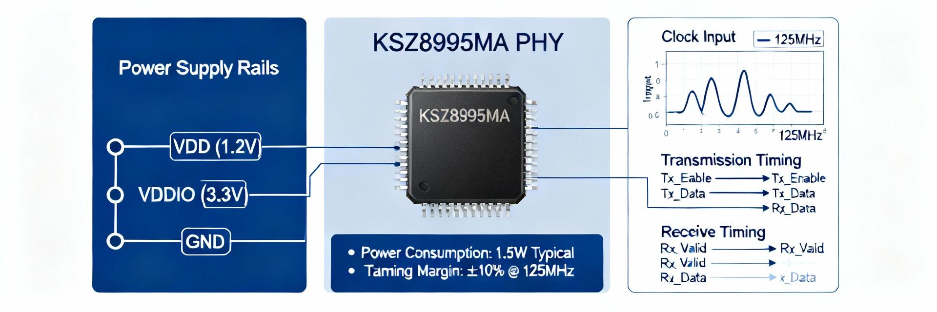
Point: Not every parameter is equally impactful. Evidence: Supply rails, quiescent and active currents, I/O voltage thresholds, drive strengths, common-mode ranges, and thermal parameters directly affect power supply sizing, PCB layout, and reliability. Explanation: Extract these into a one-page spec summary for BOM, DC/DC sizing, and thermal simulation so reviewers and BOM owners have a single reference.
H2: Key electrical specifications — voltages, currents and thermal (electrical specs)
Point: Supply and thermal items determine whether the device operates reliably. Evidence: Recommended VCC range, allowable ripple, sequencing notes, and absolute maximum voltages appear in adjacent tables. Explanation: Verify decoupling close to each VCC pin, calculate worst-case VCC ripple under peak switching, and ensure power sequencing complies with any stated ordering constraints.
H3: Supply rails, ranges and tolerances
Point: Different rails have distinct tolerances and recommended decoupling. Evidence: The datasheet lists typical VCC and Absolute Maximum ratings with ripple and ESR guidance in notes. Explanation: For each rail, verify capacitor types and placement, calculate expected voltage droop from transient currents, and ensure any required sequencing is documented in the PCB assembly instructions.
H3: Current consumption and power budgeting
Point: Use typical vs. max currents to build conservative budgets. Evidence: Tables show idle, active, and TX/RX currents with test conditions. Explanation: Sum core and PHY transmit currents, add interface loads and margin (suggest 20–30% headroom), and validate with a small sample calculation before the first build.
| Item | Typical | Design Margin | Budget |
|---|---|---|---|
| Core supply | 150 mA | +30% | 195 mA |
| PHY TX (all ports peak) | 320 mA | +30% | 416 mA |
H2: Timing, interfaces, and signal integrity (timing)
Point: Timing tables and diagrams set interface limits that affect MCU/SOC configuration. Evidence: The datasheet provides MDC clock limits, MDIO setup/hold, MII/RMII timing, and RX/TX turnaround times with diagrams. Explanation: Translate those limits into software delays, maximum clock settings, and maximum trace lengths for reliable PHY control and data transfer.
H3: PHY/MII/MDC-MDIO timing parameters to extract
Point: Extract discrete timing values for controller configuration. Evidence: MDC frequency limit, MDIO setup and hold times, and MDIO turn-around windows are tabulated with test vectors. Explanation: Configure the host MDC to a safe fraction of the stated max, implement MDIO wait loops based on worst-case hold times, and log actual MDIO cycles during bring-up to confirm behavior.
H3: I/O timing, slew, and signal-integrity considerations
Point: Rise/fall times, propagation delays, and skew affect trace layout and termination. Evidence: Data sheets show propagation delay and edge-rate guidance and sometimes recommend series resistors or terminations. Explanation: Match trace lengths where skew matters, place source termination close to driver, and use common‑mode filtering or chassis grounding when differential common-mode ranges approach limits.
H2: Example: interpreting KSZ8995MA electrical test results (case study)
Point: Walk through a concrete parameter to set design margins. Evidence: Pick an IO input threshold listed in millivolts with VCC and temperature conditions. Explanation: If the threshold is Vih = 0.7·VCC typical, recalculate at VCC minimum and worst-case temperature; choose a host drive that provides a 150–200 mV margin to account for noise and board losses.
H3: Real-world example — reading the Electrical Characteristics table
Point: Convert table entries into margin calculations. Evidence: A TX amplitude spec given at VCC and 25°C can shift with VCC tolerance and high temperature. Explanation: Apply ±5% VCC tolerance and a conservative -10% amplitude derating for high temperature, then verify that the resulting eye meets the host receiver’s sensitivity to maintain link margin.
H3: Typical bench measurements and expected deviations
Point: Typical values differ from production worst-case. Evidence: Bench measures VCC ripple, idle current, MDIO timings, and eye diagrams against table “typical” values. Explanation: Define pass/fail thresholds (e.g., current
H2: Practical design & validation checklist for engineers (actionable recommendations)
Point: A prioritized checklist shortens debug cycles. Evidence: Datasheet numbers inform decoupling, copper pour, and test steps. Explanation: Implement must-do items first (accurate decoupling, thermal vias under exposed pad, port terminations) then recommended items (series resistors, common-mode chokes) before prototype sign-off.
H3: Power, decoupling, and thermal layout checklist
Point: Place decoupling by pin and enable thermal dissipation. Evidence: Supply ripple and thermal resistance entries guide capacitor values and via counts. Explanation: Use multiple low-ESR ceramics per VCC, place them within 2–4 mm of pins, route large copper pours to the exposed pad with 8–12 thermal vias, and verify board temperature under worst-case power.
H3: Test plan and debugging priorities
Point: Structured validation finds issues quickly. Evidence: Sequence: smoke test, idle current, interface timing, PHY TX/RX. Explanation: If measured current exceeds datasheet max, isolate rails and disable ports to narrow the fault; check MDIO activity and perform simple link tests before full traffic stress tests.
H2: Summary
Point: Treat the datasheet as the single source of truth for design limits. Evidence: Voltages, currents, thermal limits and timing all derive from datasheet tables and diagrams. Explanation: Build a concise spec summary pulled from the KSZ8995MA datasheet, apply conservative margins (20–30%), and validate with the prioritized test plan to reduce spin cycles.
H2: Key Summary
- Extract supply ranges, allowable ripple, and sequencing notes from the datasheet into a one-page spec to guide BOM and thermal calculations; include margins for VCC tolerance and temperature.
- Budget power by summing core, PHY TX, and interface loads using typical and maximum currents; add 20–30% headroom and verify with bench idle and active current measurements.
- Translate timing tables (MDC, MDIO, MII/RMII) into host clock and delay settings and apply layout rules for skew, termination, and common‑mode filtering based on propagation and edge-rate specs.
H2: Common Questions (FAQ)
H3: How should engineers use the KSZ8995MA datasheet for power budgeting?
Use the datasheet’s typical and maximum current entries for core and PHY functions, add interface load currents, and apply conservative headroom (20–30%). Measure idle and active currents on a prototype to validate assumptions and adjust the DC/DC converter sizing if measured values exceed the budget.
H3: What timing parameters from the datasheet are critical for MDIO/MDC?
Extract MDC maximum clock rate, MDIO setup/hold, and turn‑around times from the timing tables and diagrams. Configure the host MDC to a safe fraction of the stated maximum and implement MDIO delays in firmware based on worst-case hold times to avoid mis-reads during register accesses.
H3: When should layout be suspected versus silicon variance if electrical specs fail?
Suspect layout when VCC ripple, ground bounce, or signal integrity issues appear (large ripple, failed eye, skew). If layout checks pass, compare multiple units; consistent deviation across units points to silicon variance or incorrect operating conditions; intermittent failures often indicate layout or assembly issues.
