Comparators are chosen by their datasheet numbers: supply range, input offset, propagation delay and output type directly govern timing, interfacing and reliability in circuits. This article extracts the LM311N critical specs and timings from the original datasheet, explains how those figures constrain real designs, and gives hands-on guidance for interfacing and troubleshooting. The goal is to turn datasheet tables and graphs into concrete design checks and bench tests.
Readers will get a concise, actionable path from reading the original datasheet to validating thresholds, calculating pull-ups, estimating switching time, and debugging real circuits. Throughout, the emphasis is practical: which table or graph to copy, which lab measurement to run, and how each spec maps to a design decision.
1 — Background: What the LM311N Is and When to Choose It
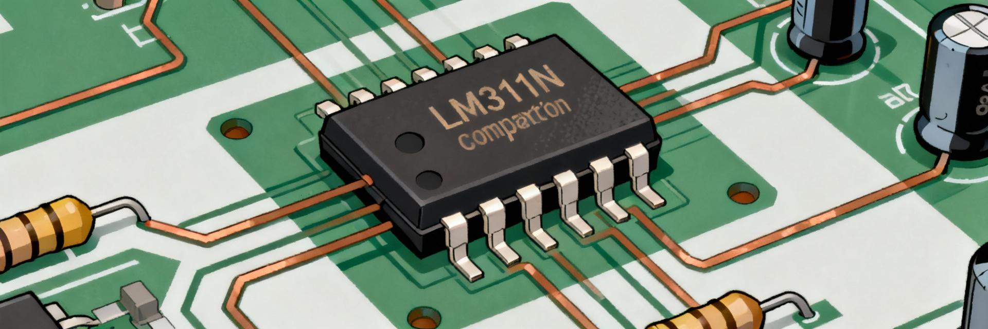
What the LM311N does and common package/pinout
Point: The device is a dedicated voltage comparator used when fast, unbuffered threshold decisions are required. Evidence: the original datasheet classifies it as a comparator and includes package/pin diagrams. Explanation: expect through-hole and small-outline packages; watch input pins, open-collector output, strobe/enable and power pins when planning board layout and isolation.
How to read a comparator datasheet (quick primer)
Point: A comparator datasheet has predictable sections that map to design checks. Evidence: look for Absolute Maximum Ratings, DC Characteristics, AC Characteristics and plots in the original datasheet. Explanation: copy Absolute Maximums for safety checks, DC tables for offset and bias, AC tables/graphs for propagation delay and rise/fall—use those tables to build a design validation sheet.
2 — Key Electrical Specs: DC Characteristics & Limits
Supply, power and absolute maximums
Point: Supply limits and quiescent current determine logic compatibility and thermal behavior. Evidence: the original datasheet lists absolute max and recommended operating ranges plus supply current. Explanation: verify that your chosen VCC fits the recommended range, ensure pull-up voltage does not exceed output transistor limits, and account for quiescent dissipation when arranging thermal margin and decoupling.
Input-stage specs: input offset, input bias, common-mode range
Point: Input offset, bias current and common-mode range set threshold accuracy and allowable signal window. Evidence: DC tables and offset vs temperature curves in the original datasheet. Explanation: translate offset plus input bias into worst-case threshold error, ensure your input signals stay inside the comparator's common-mode window, and add hysteresis if offsets or drifts approach the threshold margin.
3 — Timings & Dynamic Performance (AC Characteristics)
Propagation delay, rise/fall times and transition behavior
Point: Propagation delays and output transition times define latency and maximum toggling rate. Evidence: AC characteristic tables and timing graphs in the original datasheet list tPLH/tPHL and rise/fall under specified loads and input overdrive. Explanation: use those conditions to scale delay for your supply, load and pull-up; heavier pull-ups or larger capacitive loads increase transition time and observable propagation delay.
Slew rate, common-mode rejection at speed, and input overdrive effects
Point: Switching speed is influenced by effective slew behavior, common-mode limits and input overdrive. Evidence: timing curves and overdrive vs delay plots in the original datasheet. Explanation: estimate real-world switching time by interpolating delay vs overdrive curves; avoid designs that rely on comparator slew to meet tight analog edges—add buffering or increase overdrive where necessary.
4 — Output Stage & Interfacing: Making LM311N Work with Logic and MCUs
Open-collector output: pull-up choice and logic-level compatibility
Point: The LM311N uses an open-collector output, so pull-up selection and allowable pull-up voltage control speed and logic levels. Evidence: the output stage description and output current limits in the original datasheet. Explanation: compute pull-up value from desired rise time and allowable sink current (R = Vpullup / Ipull-up when low), balance speed versus power by selecting lower resistance for faster edges while staying within output transistor current limits.
Strobe/enable pin, output conditioning and level shifting
Point: The strobe pin permits active output disabling, useful when interfacing to different logic families. Evidence: strobe function and input thresholds described in the original datasheet. Explanation: wire strobe to MCU GPIO with appropriate pull-up/pull-down and use simple transistor or MOSFET level shifters when the pull-up voltage required exceeds MCU tolerance, always respecting input thresholds from the datasheet.
5 — Practical Circuits & Use Cases
Typical reference circuits to include and annotate
Point: Certain circuits exercise different datasheet specs—zero-cross detectors stress input range, hysteresis circuits rely on offset and bias, timing discriminators need propagation data. Evidence: design examples and recommended external networks commonly shown or derivable from the original datasheet parameters. Explanation: for each example list the specs to verify—common-mode range and output drive for zero-cross, offset and bias for hysteresis thresholds, and propagation delay plus pull-up for timing discriminators.
Real-world constraints: power, noise and temperature
Point: Power decoupling, input filtering and temperature change both DC and AC behavior. Evidence: offset vs temperature and noise plots in the original datasheet. Explanation: add local decoupling near power pins, use series resistors or RC filters on noisy inputs, and consult offset/temperature curves to decide if trimming or compensation is required for precision thresholds across expected temperature ranges.
6 — Design Checklist & Troubleshooting Guide
Pre-deployment checklist: reading the datasheet to validate design
Point: A concise checklist prevents common integration errors. Evidence: compile absolute max, DC and AC tables from the original datasheet into a validation sheet. Explanation: verify absolute maximums, confirm input common-mode for expected signals, calculate pull-up and output current, check timing for your load, add decoupling and input hysteresis—all before PCB release.
Debugging common failures and tests to run on bench
Point: Systematic bench tests isolate speed, offset and output-drive problems quickly. Evidence: typical lab measurements mirror datasheet test conditions. Explanation: swap pull-up values to test speed vs amplitude, inject slow ramps to reveal offset or built-in hysteresis, scope both inputs and output to measure tPLH/tPHL and ringing, and thermally stress the device to find intermittent behavior.
Summary
- The LM311N datasheet gives the DC and AC numbers that determine suitability for threshold, timing and logic-interfacing designs; extract absolute max, DC tables and timing graphs to build your checklists.
- Key design actions: confirm input common-mode, compute pull-up for rise time vs sink limits, and scale propagation delay from datasheet conditions to your supply and load for predictable timings.
- On the bench: measure propagation delays with known overdrive, vary pull-up values to observe rise/fall trade-offs, and consult offset vs temperature curves for robust threshold behavior.
Frequently Asked Questions
What are the most important LM311N datasheet specs to check for timing?
Check propagation delays (tPLH/tPHL), output rise/fall under specified loads, and the input-overdrive conditions used in timing plots in the original datasheet; these let you predict latency and maximum switching frequency under your pull-up and load capacitance conditions.
How should I choose a pull-up resistor for an LM311N output?
Calculate the resistor from desired rise time and permitted sink current: R = Vpullup / I_sink_max while ensuring the chosen current is within the output transistor limits shown in the original datasheet. Lower R yields faster edges but increases power and stress on the device when output is low.
What bench tests confirm LM311N timing and threshold performance?
Use an oscilloscope to capture both inputs and the output while applying a fast step or controlled ramp to the non-inverting input; measure tPLH/tPHL, vary input overdrive to map delay vs overdrive, and change pull-up values to see real rise/fall behavior—compare those results to the original datasheet curves for validation.
