Point: This quick reference compiles measured key specs that position the device as a compact, high‑isolation optocoupler for fast gate‑drive and isolation tasks. Evidence: Typical isolation rating is 5,000 Vrms, propagation delay near 200 ns, and LED forward‑current limit around 20 mA. Explanation: These values guide drive, timing margin and thermal choices during initial design scoping.
Point: Use this note to accelerate bench verification and PCB integration. Evidence: The datasheet provides the formal test conditions and derating curves. Explanation: Treat this reference as a practical companion to the official device documentation for final validation before sign‑off.
1 — Overview: What the TLP5702D4-TPET Is and Where It Fits (background)
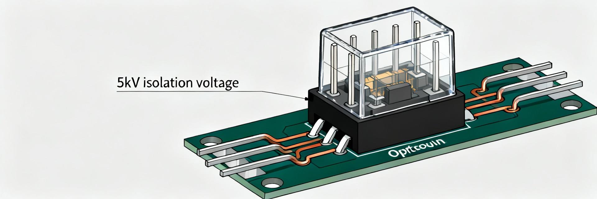
1.1 Key specs at a glance
Point: Quick technical snapshot for rapid evaluation. Evidence: Package is a 6‑pin SOIC/SO6L style, isolation 5 kVrms, If_max ≈20 mA, propagation delay ≈200 ns, output side supply examples 15–30 V, operating range −40 to +110 °C, Pd ≈40 mW. Explanation: These baseline numbers let engineers decide suitability for gate‑drive isolation and small‑signal domain separation.
| Spec | Typical / Max |
|---|---|
| Package | 6‑pin SOIC / SO6L |
| Isolation (Viso) | 5,000 Vrms |
| LED If_max | 20 mA |
| Propagation delay | ~200 ns |
| Operating Temp | −40 to +110 °C |
1.2 Typical application domains
Point: Primary use cases highlight where speed and isolation are critical. Evidence: Applications include gate‑drive isolation, microcontroller to power‑stage interfaces, small‑signal domain separation, and industrial I/O. Explanation: Fast, deterministic timing plus high isolation reduce common‑mode risk and simplify opto‑based isolation in low‑power power electronics and control paths.
2 — Quick Specs: Electrical & Thermal Parameters (data analysis)
2.1 Input (LED) electrical data
Point: LED drive sizing controls reliability and timing. Evidence: Forward voltage (Vf) typical values and If_max ≈20 mA determine resistor choices; recommended target If for long life is lower than max (commonly 5–12 mA). Explanation: Example resistor: R = (Vdrive − Vf) / If_target; for 3.3 V drive, Vf ≈1.2 V, If_target = 10 mA → R ≈210 Ω, power ≈0.021 W.
2.2 Output/isolation and thermal data
Point: Output stage limits and thermal dissipation govern derating. Evidence: Output supply ranges near 15–30 V, Pd ≈40 mW, and propagation/transition times specified under defined If and RL test points. Explanation: Read derating curves in the datasheet to apply ambient temperature and PCB thermal resistance, and size pull‑ups and snubbers to control switching stress and power loss.
3 — Pinout & Package Details — 6-pin Layout and Functions (method guide)
3.1 Pin mapping with function descriptions
Point: Correct pin mapping prevents wiring mistakes in prototypes. Evidence: Typical mapping (confirm against the official datasheet): Pin 1 = Anode (LED), Pin 2 = Cathode (LED), Pin 3 = NC, Pin 4 = GND/Output return, Pin 5 = Output, Pin 6 = Vout/pull‑up node. Explanation: Use the table below as a labeled diagram substitute and verify against the device datasheet before layout.
| Pin | Name | Function |
|---|---|---|
| 1 | Anode | LED forward drive |
| 2 | Cathode | LED return |
| 3 | NC | No connect / spacer |
| 4 | GND | Output side return |
| 5 | OUT | Open‑collector / output node |
| 6 | VOUT | Output pull‑up / supply |
3.2 PCB footprint & soldering tips
Point: Proper land pattern and reflow control preserve isolation integrity. Evidence: Use recommended land pattern with specified pad lengths, solder paste coverage and thermal reliefs; maintain creepage/clearance keepouts. Explanation: Place test points for isolation checks, use solder mask between pads to maintain creepage, and follow IPC reflow profiles to avoid package warpage.
4 — Performance Data & Measurement Tips (data analysis / method)
4.1 How to interpret CTR, propagation delay and CMRR graphs
Point: Datasheet graphs yield usable margins when read correctly. Evidence: Always note test conditions (If, RL, Vout) on CTR/td plots and consult the TLP5702 datasheet for curve axes and guaranteed ranges. Explanation: Translate typical curves to system margins by adding design safety factors for temperature, aging and manufacturing variation.
4.2 Lab test setups and verification steps
Point: Bench tests validate timing and isolation before deployment. Evidence: Key checks include LED forward‑current sweep, logic output verification, and propagation delay using a scope with clear trigger points; isolation withstand requires certified HV equipment. Explanation: Follow safe HV practices: galvanic separation, HV rated probes, and lab compliance; do not perform high‑voltage tests without proper equipment and training.
5 — Design Guidelines: Integrating the TLP5702D4-TPET in Circuits (method guide)
5.1 Biasing, protection and component selection
Point: Choose resistors and protection for reliable long‑term operation. Evidence: Drive resistors sized per R=(Vdrive−Vf)/If_target; output pull‑ups selected to meet rise time and power limits across 15–30 V. Explanation: Add transient suppression (TVS), series resistance, and decoupling to control dV/dt and clamping energy when interfacing to power stages.
5.2 Layout, thermal and reliability considerations
Point: Layout decisions affect noise immunity and longevity. Evidence: Maintain clear ground partitioning, maximize creepage distance, place decoupling close to output side supply, and account for thermal derating in dense assemblies. Explanation: Use conformal coating only after verifying creepage needs; include test coupons for assembly qualification and thermal cycle screening.
6 — Instant Reference: Troubleshooting & Pre-deployment Checklist (action)
6.1 Common failure modes and diagnostics
Point: Rapid diagnostics reduce debug cycles. Evidence: Typical symptoms: no output (open LED or incorrect resistor), slow switching (low If or heavy load), intermittent isolation breaches (contamination/creepage), thermal overstress. Explanation: Quick flow: measure LED Vf → measure If → verify pull‑up and output levels → inspect PCB for contamination or solder bridges.
6.2 Pre-deployment checklist
Point: Final validation avoids field failures. Evidence: Checklist items include confirming schematic pinout to datasheet, verifying land pattern, running timing/isolation tests, and documenting thermal derating and BOM notes. Explanation: Keep datasheet revision in the BOM, record bench results, and require production test vectors that include timing and insulation checks.
Summary
Point: The device provides compact high isolation with deterministic timing for gate‑drive and domain separation. Evidence: Key specs—5 kVrms isolation, ~200 ns delay, If_max ≈20 mA—are suitable for many control‑to‑power interfaces. Explanation: Use this reference to scope, bench‑verify and integrate, and always cross‑check the official datasheet for final design validation.
Key Summary
- Compact 6‑pin optocoupler with 5 kVrms isolation and ~200 ns propagation delay, suitable for gate‑drive and logic isolation; verify If limits and thermal Pd in your design context.
- Drive resistor rule: R = (Vdrive − Vf) / If_target; example 3.3 V, Vf≈1.2 V, If_target=10 mA → R≈210 Ω; choose lower If for longevity.
- PCB best practices: follow recommended land pattern, maintain creepage clearances, add test points, and apply reflow profiles that minimize package stress for reliable results.
Common Questions & Answers
How should I size the LED resistor for the device?
Choose R by R = (Vdrive − Vf) / If_target using a conservative If_target (5–12 mA). Verify power dissipated in the resistor and ensure If does not exceed the 20 mA absolute maximum. Document chosen values in the BOM and test at high/low temperature extremes.
What scope setup yields reliable propagation delay measurements?
Use a dual‑channel scope with one channel on the LED drive and the other on the output node; use identical probe compensation, 50 Ω termination if specified, and trigger on the rising edge at a defined threshold. Repeat tests across If and load conditions to capture worst‑case delay.
What are the safe isolation test practices before production?
Perform insulation/withstand tests only with certified HV equipment and trained personnel; maintain proper PPE, use a screened HV chamber if available, and verify creepage/clearance on the assembled PCB. Record results and rely on accredited lab testing for final regulatory compliance.
