The 0528921033 is a 10-contact, 0.50 mm pitch, right-angle ZIF FFC/FPC connector with bottom contacts and surface-mount termination; typical per-part current rating is ~0.5 A per contact. This article condenses the practical datasheet facts, exact pinout, recommended PCB footprint, assembly and reflow guidance, plus test and troubleshooting steps so engineers have a single actionable reference for integration. The goal is to make selecting, documenting, and validating the connector fast and repeatable while preserving signal integrity and mechanical reliability.
Product Overview and Use Cases
Point: The component is an FFC/FPC connector in a right-angle, zero-insertion-force (ZIF) form factor with bottom-facing contacts suitable for low-profile board-to-flex connections.
Evidence: Ten positions, 0.50 mm pitch, surface-mount body, bottom contact termination are the defining mechanical attributes.
Explanation: These traits make the part ideal where a slim edge connector and low insertion force are required for mating thin flex cables without excessive board area or tall header stacks.
- 10 contacts, 0.50 mm pitch
- Right-angle ZIF, surface-mount, bottom contacts
- Typical current rating ~0.5 A per contact
- ZIF latch for repeatable insertion/removal
Usage Context: Typical use cases include small displays, camera modules, keypad or low-speed sensor flex connections. The connector’s pitch and contact count are optimized for short flex runs carrying I2C, SPI, UART, GPIO, and low-speed differential pairs.
Critical Electrical & Environmental Specifications
Electrical Ratings
- Contact Resistance: ≤ 100 mΩ
- Insulation Resistance: ≥ 100 MΩ
- Withstanding Voltage: 200–300 V AC
Reliability & Environmental
- Temp Range: -40°C to +85°C
- Mating Cycles: 30–100 Cycles
- Finish: Tin or Controlled Alloy
- Soldering: Lead-free Reflow Compatible
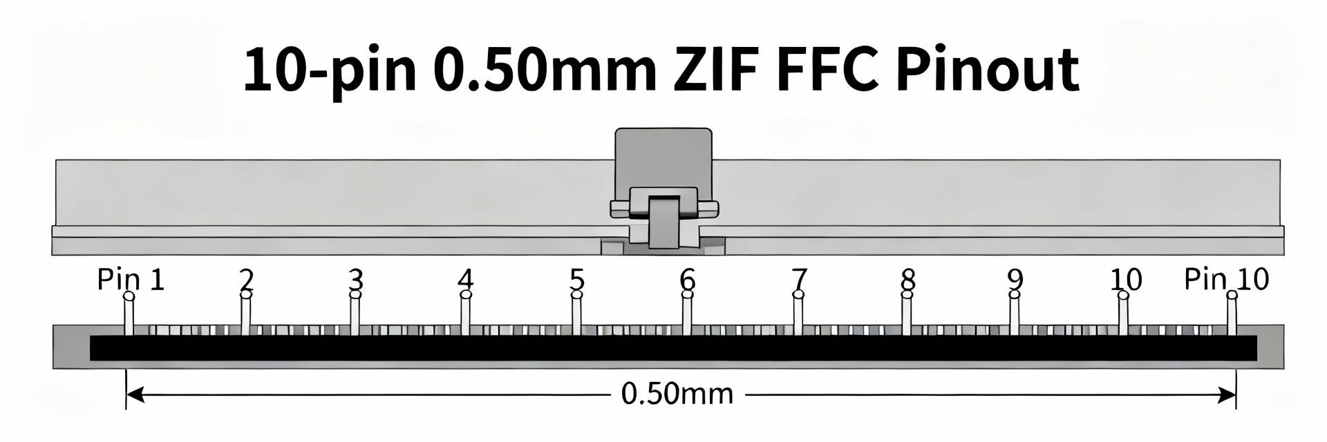
Pinout, Orientation and Connector Mechanics
Standard convention places Pin 1 at the left-most contact when the marked end of the connector faces up and the cable inserts toward the board. Documenting this map is critical to avoid assembly errors.
| Pin Number | Function (Example Implementation) | Signal Type |
|---|---|---|
| 1 | SDA / Signal 1 | Digital I/O |
| 2 | SCL / Signal 2 | Clock |
| 3 | GPIO / Signal 3 | General Purpose |
| 4 | GND | Reference |
| 5 | VCC (Power, Low Current) | Power Supply |
| 6 | NC / Reserved | No Connect |
| 7 | RX / Signal | UART RX |
| 8 | TX / Signal | UART TX |
| 9 | CLK / Signal | High Speed Clk |
| 10 | Shield / Optional Ground | EMI Shielding |
PCB Footprint, Land Pattern & 3D Model Guidance
Recommended Land Pattern: For 0.50 mm pitch bottom contacts, typical pad recommendations use rectangular pads centered on pitch with:
~0.7 mm
~0.3–0.35 mm
~50% Aperture
Clearance & 3D: Place a mechanical keepout around the mating area to prevent tall components from obstructing the cable. Typical cable bend radius recommendations aim for no less than 5–8 times the flex thickness near the connector.
Assembly, Soldering and Test Checklist
A standard Pb-free reflow envelope with peak temperatures up to 245–260°C for 20–40 seconds is recommended. Avoid excessive localized heat when hand-soldering to prevent deforming the plastic latch.
| Pin # | Expected Connection | Target Resistance |
|---|---|---|
| 1 - 3 | Continuity to harness (Signals) | |
| 4 | Continuity to board GND | |
| 5 | VCC Present (if fitted) |
Key Summary
- Essentials: 10 contacts @ 0.50 mm pitch, right-angle ZIF. Design for 0.5 A/contact.
- Footprint: Use 0.7x0.3mm pads with 50% paste reduction to prevent bridging.
- Documentation: Always mark Pin 1 on silkscreen and provide a clear schematic map.
- Validation: Run a continuity matrix and measure contact resistance (≤100 mΩ).
