Key mechanical and electrical parameters in the 0524653071 datasheet determine PCB land pattern accuracy, signal integrity, and assembly yield. For layout and test engineers, the correct interpretation of pinout, pad geometry, and seating plane tolerances directly affects first-pass success and solder reliability.
Part Background & Quick Overview
Part Function & Typical Applications
The component is a board-mount interconnect designed for reliable electrical contact in compact systems. Typical applications include board-to-board or cable-mate interfaces in industrial and consumer products. Application context—mechanical mating forces, expected current loads, and shielding—steers pinout grouping and footprint choices to ensure mechanical retention and consistent solder joints.
Identifiers to Confirm
- Package code & Full part number verification
- Revision/Version control & ordering suffixes
- 3D model availability for mechanical interference checks
Electrical & Mechanical Specification Highlights
Key Electrical Specs
Extraction of rated voltages, currents, and contact resistance is critical for trace design.
Mechanical Dimensions
| Pitch Tolerance | ±0.05 mm |
| Seating Plane | ±0.1–0.2 mm |
| PCB Thickness | Standard (1.6mm) |
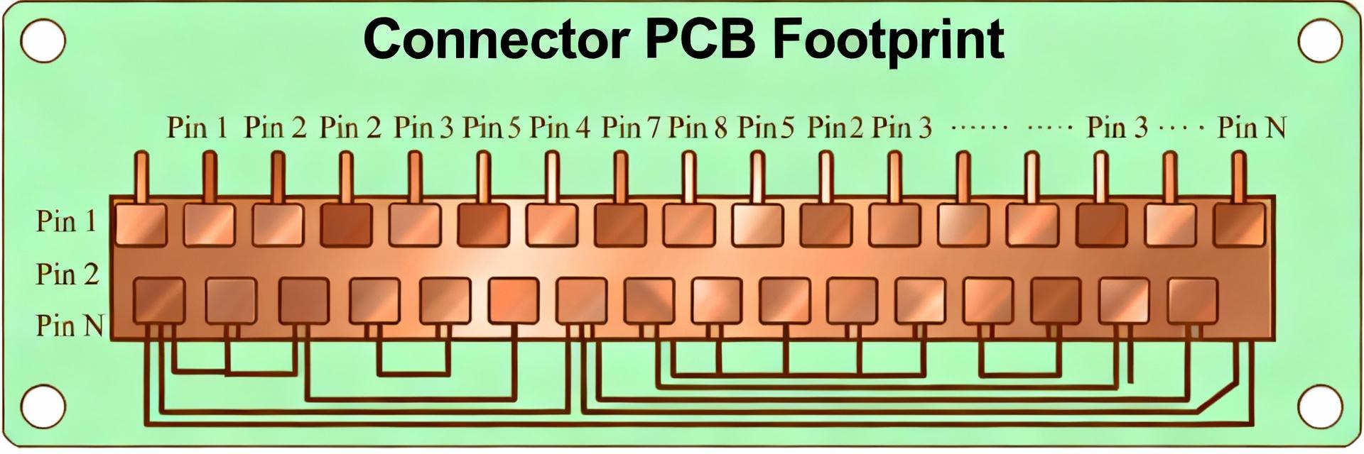
Pinout Breakdown & Signal Mapping
Numbering Convention
Use the datasheet’s view orientation (top or bottom view) to map pin numbers to your schematic symbol and PCB. Clearly mark orientation markers on silkscreen and include pin-1 reference. Label nets with function and add test-point IDs; consistent naming (e.g., PWR_VIN, GND_CONN, TX+, RX−) simplifies debugging.
Functional Grouping
Anchor points near mechanical mounts improve in-circuit test stability during probing and ATE fixtures.
Footprint & PCB Land Pattern Details
Land Pattern Derivation
Derive pad shape from 2D drawings. Use oval or rectangular pads per pin geometry and maintain a clear courtyard. Prioritize the datasheet mechanical drawing for compliance over generic vendor CAD models.
Solder Mask & Paste
Specify paste aperture reductions (typically 60–90%) to mitigate bridging. Avoid via-in-pad unless plated and filled. Provide thermal reliefs for large ground pads.
Layout, Assembly & Validation
| Phase | Best Practice Action | Expected Outcome |
|---|---|---|
| PCB Layout | Orient to match assembly flow; short & wide power traces. | Minimal solder pooling; low impedance. |
| Assembly | Validate reflow profiles against thermal limits. | Prevention of component warping or damage. |
| Validation | Perform X-ray for hidden joints; first-article inspection. | High yield; elimination of bridging/shorts. |
Pre-production Checklist
Verify footprint and stencil files against datasheet revision.
Confirm test points placed for all high-value nets.
Document assembly tolerances and acceptance criteria.
Reconcile 2D drawings with 3D STEP/IGES models.
Summary
- • Locate crucial pad and seating-plane dimensions in the 0524653071 datasheet 2D mechanical drawing; prioritize these for compliance.
- • Avoid common pitfalls: undersized pads, missing orientation markers, and inadequate thermal reliefs.
- • Immediate actions: verify datasheet + 3D model, print a physical template for fit check, and run first-article assembly validation.
