The 052271-0479 is a compact 4-contact FFC/FPC board connector commonly used where 1.0 mm pitch, roughly 500 mA per contact capability, and a -40°C to +85°C operating window are required.
Headline attributes make it a frequent choice for low-power display and camera ribbons. This article decodes the datasheet into actionable guidance.
Background & Part Overview
What this connector is
The part is a low-profile SMT FFC/FPC board connector in a ZIF (Zero Insertion Force) style with bottom contacts and right-angle entry, presented in a 1.0 mm pitch and four contacts. Plotters and handheld designs select this class for small cable counts and low stack height. As an SMT ZIF FFC connector, it requires accurate pick-and-place registration and gives the assembly benefit of tool-free cable insertion while minimizing board real estate.
Typical Applications
Tiny footprint for compact enclosures.
Reliable mating with thin flex cables.
Low insertion force for manual builds.
Full Specifications Breakdown
The 052271-0479 datasheet lists critical electrical and mechanical constraints. Treating the datasheet as a checklist avoids oversights such as undersized power traces or incompatible solder processes.
| Category | Specification Parameter | Design Action |
|---|---|---|
| Electrical | 500 mA per contact / Gold Plating | Size traces for thermal margins |
| Mechanical | 1.0 mm Pitch / Right-Angle Entry | Verify cable bend radius keepouts |
| Environmental | -40°C to +85°C Operating Range | Confirm conformal coating limits |
| Durability | 30 Mating Cycles (Typical) | Limit cycles in production testing |
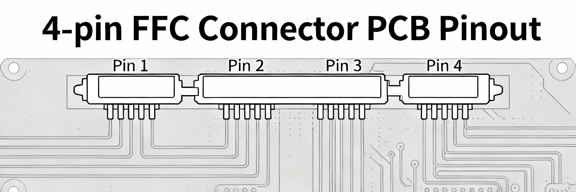
Pinout & Pin Functions
Orientation Guidance
Pin 1 conventionally sits at one end of the connector body; the datasheet drawing shows the polarity marker and bottom contact orientation. Mapping mistakes arise when designers assume top contacts or reverse numbering relative to the cable.
Routing Recommendations
- • Route power traces with at least 2× the width of signal traces.
- • Place a local ceramic decoupler within 5 mm of the power pad.
- • Keep differential pairs short with controlled impedance.
PCB Footprint & Assembly
Land Pattern Design
The PCB land pattern must reflect pad length for a reliable solder fillet. Design pads with a modest fillet length (0.6–0.8 mm), avoid solder mask between pads, and include a small mechanical anchor area if the assembly experiences vibration.
Soldering & Reliability
Use a standard lead-free reflow profile with controlled soak limits. Set inspection points for fillet shape and pad wetting. For hand soldering, avoid molten solder near the housing latch to prevent mechanical jamming.
Troubleshooting & Quick Reference
Common Failure Modes & Fixes +
Top failures: Reversed cable orientation, insufficient solder fillet, and improper mating retention.
Fixes: Add clear silkscreen orientation markings, enlarge pad length for wetting, and specify ionic-clean assembly processes.
Sourcing & Equivalent-Part Checklist +
When selecting alternates, verify pitch (1.0mm), contact position (bottom), current rating, and housing height. Run a single-mate test to confirm mechanical behavior before qualifying a supplier change.
Integration Case: Camera Module +
Reserve one contact for ground and one for primary power. Use the two remaining contacts for clock/data. Add a mechanical standoff to constrain lateral movement and reduce intermittent contact risk.
